In today’s digital world, the extensive use of electronic devices and accelerating use of AI drive demand for a diverse range of chip types, including GPUs, CPUs, ASICs, DRAM, NAND, power devices and more. The latest smartphones can have more than 180 chips, and a smart vehicle can have over 6,000 semiconductors. A single, leading-edge AI chip is a complex, multi-chip package with large, leading-edge design node GPUs and eight or more high bandwidth memory (HBM) chips, each containing eight or more DRAM chips. That one AI chip package depends on the quality of more than 65 individual chips – and there are many of these AI chips in a server, and numerous servers in a data center.
Click below for easy navigation:
Sub-Resolution Sensitivity and Speed
BBP Technology Innovations
BBP’s Role in Chip Manufacturing
KLA’s BBP Inspectors
This widespread use of semiconductors means the quality of our electronics and digital experiences depends on the quality of the chips, resulting in an increased focus by manufacturers on chip performance, yield and reliability.
Additionally, the production of advanced logic and memory chips involves ever-shrinking design nodes, new technologies (EUV lithography, advanced packaging, etc.) and novel architectures (gate all around (GAA) transistor, backside power delivery, etc.). These chip innovations create production challenges that must be addressed to achieve quality targets.
Process control – inspection and measurement of product at various steps in the manufacturing process – serves a key role in helping chipmakers identify issues that can affect final chip quality. As part of a chipmaker’s process control strategy, wafer inspection is used to detect critical defects of interest (DOI) after specific process steps, helping fab engineers resolve critical process excursions.
Broadband Plasma (BBP) Inspection System – KLA Flagship Product
Our broadband plasma (BBP) patterned wafer inspection systems are the flagship product in our comprehensive inspection portfolio. BBP inspectors use advanced optical and data processing technologies to discover critical defects on patterned wafers during chip manufacturing. With tunable broadband illumination, flexible operating modes and multiple models, BBP inspectors support defect characterization and monitoring across the process layers, device architectures and design nodes used to produce today’s diverse chip types.
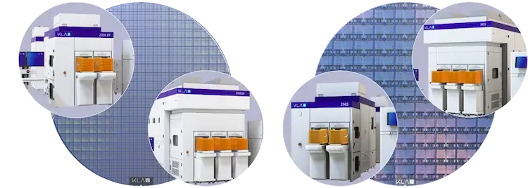
Our latest broadband plasma inspection systems include the 3935 Super Resolution Broadband Plasma patterned wafer Defect Inspection System and 2965 Broadband Plasma Patterned Wafer Inspection System for advanced foundry and leading-edge logic manufacturing, the 3920 EP and 2950 EP for advanced memory manufacturing and the C30x for advanced legacy chip manufacturing. (Find more information about our current inspectors below.)
Additionally, we continue to develop innovations that extend our BBP optical inspection platforms to support the industry’s advancements in chip technology. Our next-generation BBP platforms are currently being evaluated by our customer partners for defect detection capability on the most advanced logic and memory devices and architectures. (We look forward to sharing more about these new BBP inspectors soon.)
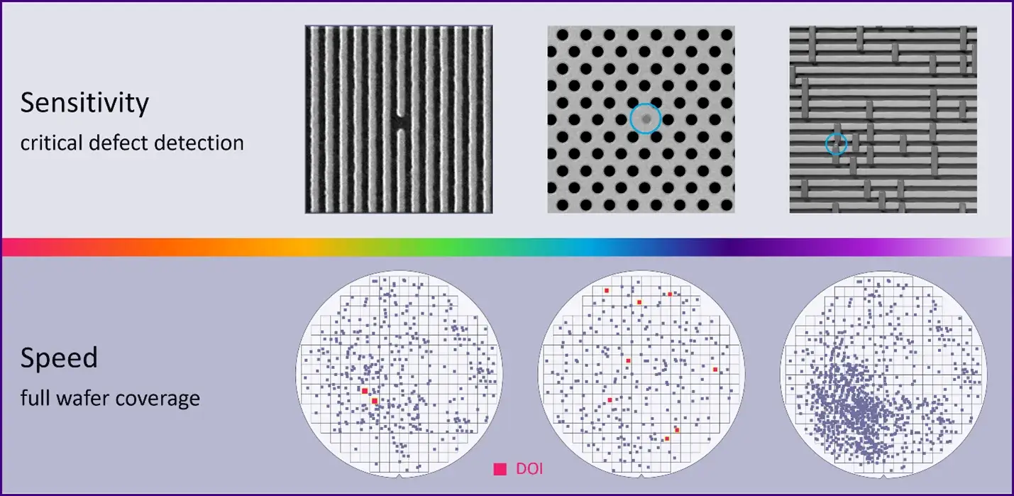
Broadband Plasma Sub-Resolution Sensitivity and Speed
BBP inspectors are a unique class of optical patterned wafer inspection systems that deliver high sensitivity at the inspection speeds needed for fast defect learning cycles during R&D and inline excursion monitoring during high-volume manufacturing. Broadband plasma inspector sensitivity supports detection of a wide range of defect types and sizes, including nanoscale defects on leading-edge design node devices. The speed of BBP inspectors facilitates coverage – full wafer inspection is critically important because significant DOI can occur anywhere, and wafer-level signatures deliver important information for the characterization of process issues.
Broadband plasma inspectors operate by using broadband light to scan a wafer in a serpentine pattern. The reflected images are collected by high data rate sensors. High-performance image computers, which use custom GPU architectures, perform real-time image analysis to extract anomalous pixels that correspond to defects. The BBP inspector outputs defect information, including defect locations mapped to coordinates on the wafer and other key defect attributes.
One of the main technological advantages of BBP optical inspection is that a defect doesn’t have to be resolved to detect it. During image analysis, an image from a small area of a chip on the wafer, the target image, is compared to a reference image generated from the same location in nearby chips.
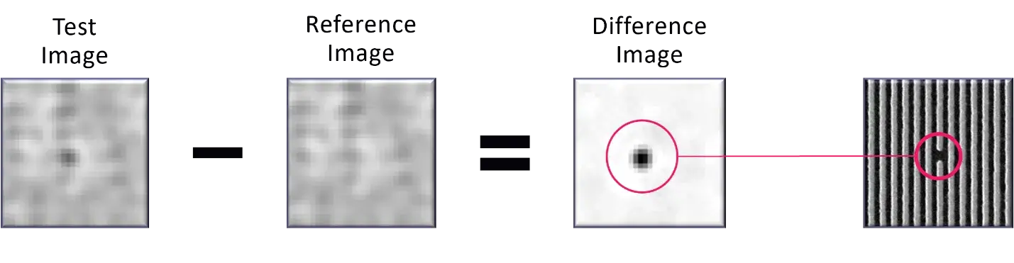
These images don’t need to resolve the patterns on the wafer or any defects. The resulting difference image just needs a pixel to be slightly different than the surrounding pixels in order to flag a potential defect. This means that BBP inspectors can use illumination wavelengths that are 20 times larger and pixel sizes that are at least two times larger than the sizes of defects being found. Through sub-resolution defect detection, BBP optical inspectors provide the sensitivity to consistently find relevant defects at the speeds that support inline monitoring requirements for advanced design nodes.
Broadband Plasma Technology Innovations
BBP inspectors employ multiple technologies to maximize the defect signal-to-noise ratio – the contrast between a defect and its surroundings. By leveraging the flexibility of these technologies, the BBP inspectors achieve maximum sensitivity to critical defects across a range of process layers, device types and design nodes.
Broadband Plasma Illumination
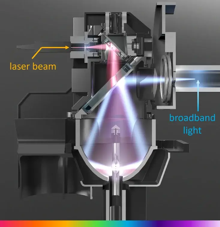
BBP inspectors derive their name from their industry-unique, broadband plasma illumination source. A laser is used to ignite a plasma that produces light that covers a range of wavelengths. The light generated is very high brightness, delivering strong signal on small critical defects.
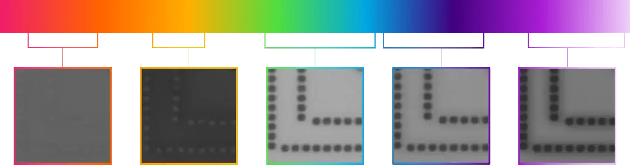
Tunable Wavelength Bands
The broadband light produced by the illuminator can be tuned to specific wavelength ranges. The wavelength band used for inspection affects the contrast of the images generated by the BBP inspector, and the best wavelength band to use for inspection varies by process layer and defect type. The flexibility afforded by wavelength tunability facilitates detection of a range of defect types across different process layers and device types.
Optical Innovations
High numerical aperture (NA), large field-of-view optics, selectable optical apertures and multiple pixel sizes produce optimal defect signal, reduce wafer noise and offer flexibility to detect a wide range of defect types.
TDI Sensor
A very low-noise, high-sensitivity TDI (time delay integration) sensor operates at high data rates, supporting the inspection speed needed for fast defect learning cycles and inline monitoring applications.
Data Processing
High data rate image computers with custom GPUs process inspection data in real time, delivering a population of defects that affect chip quality, yield and reliability.
Advanced Algorithms
Custom defect detection algorithms produce actionable data on critical defect types. They cover a range of capabilities, including suppression of noise related to pattern or process variations, accurate binning of defects and improved capture of defects in critical die areas.
Broadband Plasma’s Role in Chip Manufacturing
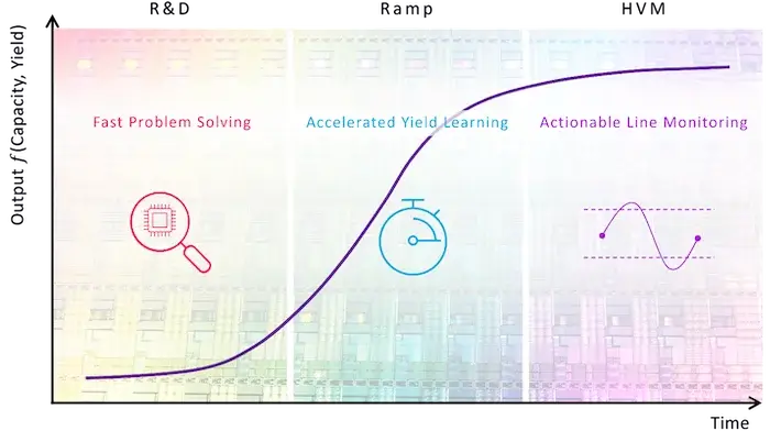
Our broadband plasma patterned wafer inspection systems are used by foundry, logic and memory manufacturers to detect defects that affect the yield, reliability and performance of chips. BBP inspectors are used by chip manufacturers through all stages of manufacturing. By discovering systematic defects, the BBP inspectors deliver comprehensive defect information to chip manufacturers during R&D, helping speed characterization and optimization of new processes, design nodes and device architectures. During ramp, the BBP inspectors help reduce baseline defectivity and accelerate yield learning by quickly finding process excursions. During high-volume manufacturing, the BBP inspectors leverage high defect sensitivity at optical inspection speed to deliver accurate, actionable data for effective line monitoring.
Chipmakers rely on the sensitivity, speed and flexibility of broadband plasma inspectors for the following defect inspection applications used during various stages of chip production:
- Defect discovery: characterization and debug of defect issues encountered during new process development
- Inline monitoring: identification of defect excursions related to process anomalies that affect final chip quality
- Final check: defect monitoring at the final step of each process module (CMP, etch, etc.) to ensure the module is producing wafers free of critical issues
- PWQ: detection of process-induced defects on an intelligent wafer layout for accurate process window discovery and qualification
- EUV Print Check: detection of repeater defects to qualify EUV reticles during production
KLA’s BBP Inspectors
Our new broadband plasma optical inspectors include the 3935, 3920 EP, 2965, 2950 EP and C30x. These systems offer the inspection flexibility to support production of the vast array of chip types produced for today’s digital world. Advancements in the BBP core technologies (e.g., tunable broadband illumination source, high-data-rate sensor and image computer, advanced algorithms) extend the inspection performance of these new BBP models, enabling discovery of critical defects during production of the latest chip designs.
The 3935 and 2965 BBP inspectors are used in advanced foundry and logic manufacturing, while the 3920 EP and 2950 EP inspectors support advanced DRAM and 3D NAND memory manufacturing. Through systematic defect discovery and inline monitoring, the 29xx and 39xx inspectors ensure quality production of the GPUs and DRAM chips needed for AI, and the CPUs and 3D NAND chips used in smartphones, personal computers and other electronics.
With complementary wavelength bands – DUV/UV/visible on the 29xx Series and super-resolution DUV (SR-DUV) on the 39xx Series – the systems cover inspection applications across a range of advanced design nodes, process layers and device types.
All 29xx and 39xx models include multiple technologies that produce actionable data on critical defect types through efficient suppression or separation of nuisance defects, including iDO™ 3.0 with advanced machine learning techniques.
Additional key innovations integrated on these advanced BBP defect inspectors include:
- The 2965 features a unique wavelength band that enables capture of critical nanosheet defects, helping logic/foundry chip manufacturers to ramp and produce leading-edge chips, such as GPUs for AI applications, with GAA transistor architectures.
- The 3935 and 3920 EP include wavelength bands that make them particularly suited for EUV lithography quality control applications, including print check for reticle requalification and after-develop inspection (ADI).
- The 2965 and 2950 EP feature Super•Pixel™ inspection test mode for high-sensitivity inspection at optimal cost of ownership.
- Available as an option on the 3935, DualSENS™ technology provides seamless linkage between the 3935 optical inspector and e-beam defect review systems for enhanced defect verification on low-contrast defects.
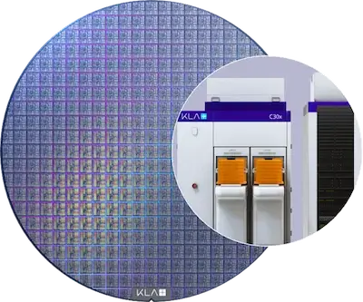
The C30x Series BBP inspectors support production of larger design node chips used in automotive, IoT, 5G, consumer and industrial markets. The C30x inspectors leverage a tunable broadband illuminator, selectable optics and pixels sizes, a low noise sensor, NanoPoint™ technology and advanced algorithms for systematic defect discovery and latent reliability defect detection.
With these technologies, the C30x Series inspectors deliver actionable defect data that helps improve chip reliability and reduce die underkill and overkill, supporting the chip quality requirements of the automotive and other industries.
The future is bright for our broadband plasma optical patterned wafer inspection platform. Our engineers and scientists continue to develop innovations across all of our core technologies (light, sensor, compute, algorithms, etc.) that extend BBP’s optical sensitivity and speed for inspection of future design nodes and chip architectures. New platforms are coming soon, and we will share details about their detection capabilities for leading-edge transistor architectures and advanced memory devices.
Follow Us