Product Description
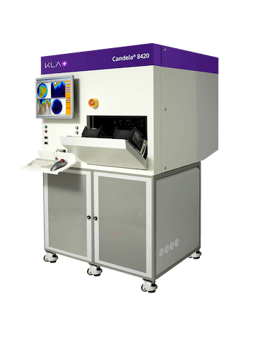
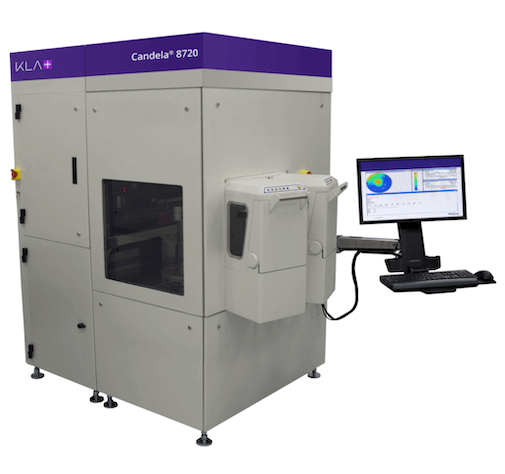
The Candela 8520 surface inspection system employs proprietary optical technology to simultaneously measure scatter intensity at two angles of incidence. It captures topographic variations, surface reflectance, phase shift and photoluminescence for automatic detection and classification of a broad range of defects of interest (DOI). The 8520 provides surface and photoluminescence defect inspection for GaN wafers, detecting and classifying GaN dislocations, pits and holes for GaN reactor defect control. Its power applications include SiC based transparent wafer inspection and classification of crystal defects such as BPDs (Basal Plane Dislocations), micropipes, stacking faults, bar stacking faults, grain boundaries, and threading dislocations. Detection of topographic anomalies include triangle detection, carrot defects, downfall and scratches.
Features
- Detects surface defects on Wide Band Gap materials including SiC and GaN (substrate and epitaxy) up to 200mm in diameter
- Supports a wide range of wafer thickness
- Detects particles, scratches, cracks, stains, pits, bumps, KOH etch mapping, carrots and surface triangles, basal plane dislocation, stacking faults, grain boundaries, threading dislocations and other macro epitaxial disturbances
Use Cases
- Substrate quality control
- Substrate vendor comparison
- Incoming wafer quality control (IQC)
- Outgoing wafer quality control (IQC)
- CMP (chemical mechanical process) / polishing process control
- Wafer clean process control
- Epitaxy process control
- Substrate to epitaxy correlation
- Epitaxy reactor vendor comparison
- Process tool monitoring
Industries
- SiC and GaN power devices
- Other high-end compound semiconductor devices
Options
- SECS-GEM
- Light tower
- Diamond scribe
- Calibration standards
- Offline software
- Optical character recognition (OCR)
- Photoluminescence


