Advanced ICs
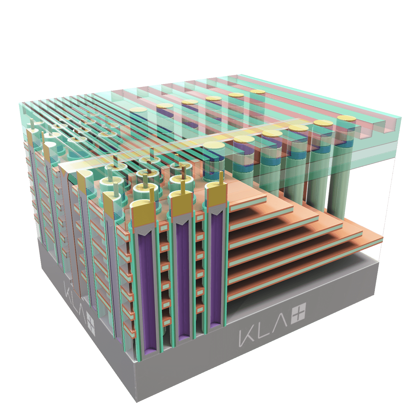
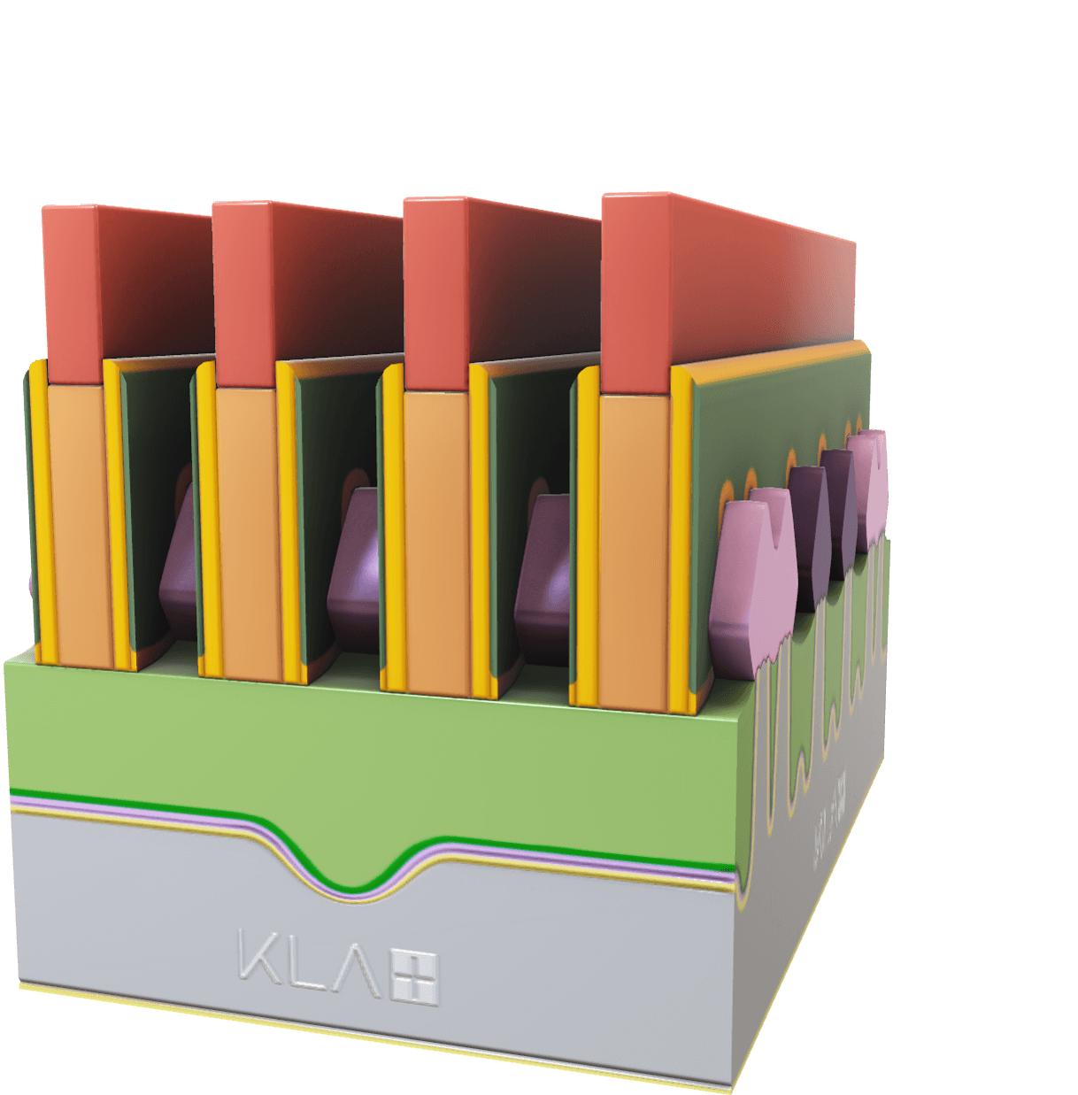
AI, 5G, cloud and edge computing, autonomous vehicles, mobile devices. Today’s electronics and tomorrow’s technologies require leading-edge GPUs, CPUs, DRAM and 3D NAND chips. These ICs are fabricated using intricate shapes and new materials, with structures that are smaller, narrower, taller and deeper. This complexity demands control of patterning anomalies to ensure manufacturing success.


Meet the Family
Our metrology solutions provide precise measurement of pattern dimensions, film thicknesses, layer-to-layer alignment, pattern placement, surface topography, wafer geometry and in situ processes. This portfolio of innovative systems helps chip manufacturers maintain tight control of their fab-wide processes, including EUV lithography, for improved performance of logic, DRAM and 3D NAND devices.
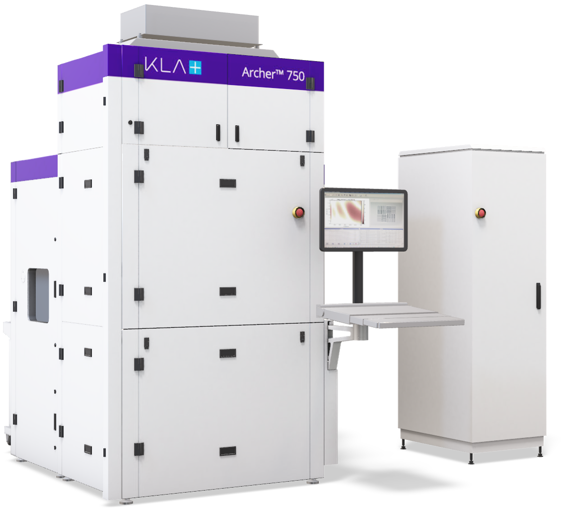
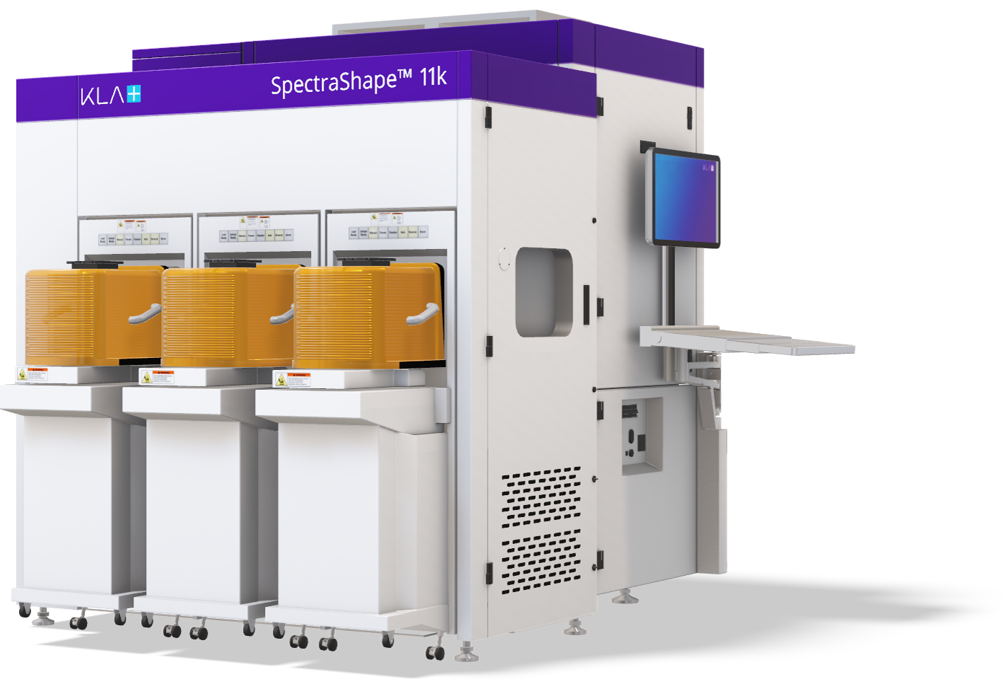
Joining the family are the Archer™ 750 and SpectraShape™ 11k! With multiple optical and platform innovations and advanced machine learning algorithms, these new systems facilitate measurement and control of critical patterning parameters, helping IC engineers achieve exceptional patterning specifications.

Click for an interactive experience
Archer™ 750
Our new imaging-based overlay metrology system provides accurate, fast measurement of overlay error, helping lithographers identify inline excursions and improve patterning performance.
- Unique wavelength tunability with 10nm resolution delivers accurate and robust overlay error measurements in the presence of process variation for fast technology ramps and stable production of advanced logic and memory devices
- New CPL (color per layer) measurement mode enhances target signal-to-noise for accurate overlay measurements on challenging lithography stacks, EUV thin resists and opaque films
- Hardware advancements, including a new stage and sensor, boost system productivity to levels typically only seen with scatterometry-based overlay systems for increased overlay sampling that supports high order scanner corrections and high volume manufacturing
- Advanced new algorithms with novel rAIM® overlay target design provide improved device to target correlation and better process robustness for improved tracking of device overlay performance

Click for an interactive experience
SpectraShape™ 11k
Our latest CD and dimensional shape metrology system provides high precision, high sampling measurement of critical device features for production monitoring of advanced IC processes.
- Significant advances in light source, polarization, stage and other subsystems support measurement of critical device features at high sensitivity and throughput for quick identification of process issues in volume production
- Fast Multi Angle (FMA) enables simultaneous data collection from multiple illumination angles at high signal intensity for measurement of challenging process parameters and layers at improved sensitivity and speed compared to the previous-generation SpectraShape system
- An extended infrared wavelength range, high-resolution reflectometer and new chuck that accommodates high bow wafers enable measurement of thick hardmask and thick film stack parameters, such as high aspect ratio channel hole etch CD, height and recess, for monitoring and control of advanced DRAM and 3D NAND processes
- TurboShape™ algorithms facilitate measurement of CD and shape at litho ADI for implementation of new scanner control or etch process control strategies that improve patterning performance


