Extreme ultraviolet (EUV) lithography is a key technology inflection for the semiconductor industry. While shifting the scanner wavelength to EUV has enabled printing of the smaller pattern features required for ≤5nm design node chips, it has also added tremendous complexity to the equipment, reticles, resists and other infrastructure required to support EUV lithography.
New defect mechanisms and tighter patterning and overlay requirements have driven the need for intensive process control strategies as EUV has moved from development to pilot to production. With EUV now in production for critical layers of logic chips and beginning to be adopted for DRAM manufacturing, process control systems are being used to monitor and control all aspects of the EUV lithography ecosystem. One of the more crucial areas of EUV process control is validating the state of EUV reticles.
Reticles, also known as photomasks or masks, contain the pattern information for features printed on wafers. Within a EUV scanner, EUV light reflects from the reticle surface, transferring the pattern from the reticle to the wafer surface. If there is a defect on a reticle, it can potentially print in every chip on the wafer, creating what is called a repeating defect. If a reticle defect results in a repeating pattern error that kills the chips, it can be catastrophic to yield. It is this potential for high-impact yield excursions that makes EUV reticle quality control so critical.

EUV reticle quality control begins during the fabrication of the reticles in mask shops and continues forward to reticle use during chip production. As the cornerstone of understanding reticle quality, reticle inspection systems find the defects that can have a devastating impact on every wafer printed.

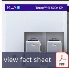
Our new, high-performance Teron™ SL670e and Teron™ SL670e XP EUV reticle inspection systems are used during chip manufacturing to identify yield-critical defects on EUV reticles. The Teron SL670e supports 7nm/5nm logic production, and the Teron SL670e XP supports 5nm/3nm logic production; both systems support advanced DRAM chip production. Key applications for these Teron inspectors include:
- Incoming quality control (IQC) of EUV reticles. The Teron SL670e and Teron SL670e XP validate that the EUV reticles shipped from reticle manufacturers to the fab are free of particle and other potentially printable defects before they enter the chip manufacturing production stream.
- EUV reticle requalification. After multiple cycles of production use, the Teron inspectors produce actionable data on particle adders and other contamination so that the reticles can be accurately dispositioned for cleaning/repair or for continued production use.
The Teron SL670e and Teron SL670e XP reticle inspectors complement KLA’s unique wafer print check solution, also used by chip manufacturers to verify EUV reticle quality during production. With print check, wafers are inspected after exposure by the scanner to find printed repeater defects that point to the presence of defects on the reticle. Reticle inspection and wafer print check form a comprehensive solution that facilitates high frequency EUV reticle quality checks that minimize yield risk at optimal cost.
KLA’s team of engineers developed state-of-the-art technologies that provide the Teron SL670e and Teron SL670e XP systems with the performance required to accurately assess EUV reticle quality. The Teron systems achieve high sensitivity to critical defects through advances in thermal stability, focus tracking and imaging flexibility, and the integration of EUVGold™ and EUVMultiDie algorithms. The Teron SL670e and Teron SL670e XP also have industry-leading production throughput, supporting the fast cycle times needed to qualify reticles during high-volume chip manufacturing.
The Teron SL670e and Teron SL670e XP join our family of advanced inspection, metrology and data analytics systems that detect, identify and source critical reticle defects and pattern placement errors during reticle blank, reticle and chip manufacturing. Covering the full range of quality control applications, KLA’s comprehensive portfolio produces information that helps reticle and chip manufacturers reduce yield loss. For more information, visit our reticle solutions page.
Follow Us

