The semiconductor industry is poised for extraordinary growth in the years to come, and innovation is at the core of it. Innovation requires collaboration across industry partners.
Ideas are only as good as their impact, and ultimately, our customer collaborations are about turning constellations of ideas into new technologies customers can use to drive their products forward. Events like SPIE Advanced Lithography + Patterning create an amazing forum for the industry to come together to share challenges and breakthroughs – and brainstorm ideas that drive innovation.

president, Semiconductor Process Control

The SPIE 2024 event was held late in February, where EUV production implementation and high numerical aperture (NA) EUV readiness were among the key themes. We also had broad discussions on innovations like new front-end architectures and advancements in packaging technology.
Technical presentations at these events create common ground for discussions that often result in solutions for some of the most complex problems facing our industry.
Many interactions highlighted the critical role metrology, inspection and process control plays in driving industry roadmaps. In fact, the process control section was the largest conference at the symposium.
KLA employees and several customers shared almost 30 papers across a range of topics such as software solutions, metrology and advanced packaging. (Links to several abstracts are included below.)
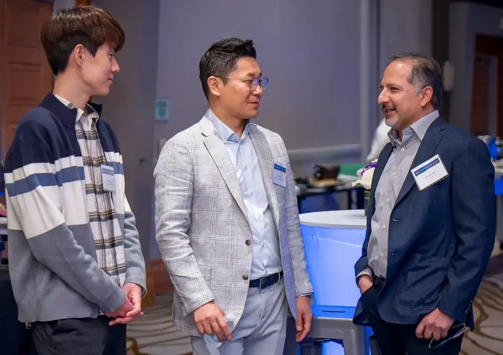
“Our engagements with peers and colleagues at events like SPIE Advanced Lithography + Patterning can spark new ways of thinking and improve on ideas that move us forward. I interacted with multiple customers at KLA Interconnect – the industry event we host at SPIE.”
Ahmad Khan
Whether engaging in casual face-to-face conversations or in more formal settings at the conference, forums like these allow us to bring meaningful ideas and innovations to the surface. This gives us room to think big, but keeps us grounded as a community, eventually narrowing our focus to the ideas that have the most relevant commercial applications.
For KLA customers, events like the SPIE Advanced Lithography + Patterning conference are yet another opportunity to visit and interact with our engineering and product teams to discuss their requirements and preview our product roadmaps. We hosted multiple customers during the week of SPIE, and I am confident that the interactions we had with industry partners, peers and customers will help drive the industry and KLA to the next phase of growth.
Below is a sampling of abstracts KLA leaders shared at SPIE Advanced Lithography + Patterning in 2024.

- Houssam Chouaib, KLA Milpitas, California, “Novel ellipsometry-based machine learning technique for characterization of low sensitivity critical dimensions within gate-all-around transistors”; proposes a methodology that uses a physical model assisted machine learning (ML) algorithm applied to the Mueller Matrix elements of spectroscopy ellipsometry to measure low-sensitivity CDs for inline monitoring of gate all around nanosheet transistor devices
- Donghwan Son, KLA Milpitas, California: “Wafer printability simulation of EUV mask defects using mask SEM and AFF”; shows how measured SEM and AFM images are processed to fit with rendered reference SEM and AFM images and how advanced scanner simulation models can determine wafer printability of mask absorber defects, buried defects and absorber residues
- Vinayak Pandey, KLA Arizona, “Process control challenges in 3D packaging”; discusses new process control solutions being developed for advanced 3D packaging
Follow Us