The KLA Instruments™ portfolio of optical profiler tools are widely used in the industry due to their rapid measurement time and ability to provide 3D topography across many surface types. One of the more challenging measurements for a traditional optical profiler is the measurement of multi-dimensional, multi-material surfaces that provide varying levels of reflectivity. When a single sample contains both very low reflectivity surfaces and high reflectivity surfaces, measurement becomes a challenge as a much smaller amount of light reaches the optical sensor from a lower reflectivity surface than it does for a higher reflectivity surface. Similarly, very rough, or very sloped surfaces also limit the amount of reflected light reaching the optical sensor making simultaneous measurement of these surfaces difficult.
New Generation Profilm3D Measures Larger Variations on a Single Surface With Fine Detail
The newest generation of the Filmetrics Profilm3D optical profiler is designed to specifically address the above mentioned challenges where larger variations in surface topography and reflectivity require resolution of fine detail. The Profilm3D is uniquely suited for applications like these because the combination of new optical techniques enables measurement with a single tool requiring no change in setup. In this feature, we highlight the applications and benefits of two such optical techniques available on the new Profilm3D – the Enhanced Roughness Mode and TotalFocus™ Imaging.
Enhanced Roughness Mode (ERM)
A drawback to using traditional white light interferometry (WLI) for measurement of rough surfaces is a low fringe contrast leading to a low signal-to-noise ratio. Phase shifting interferometry (PSI), another technique traditionally used to measure rough surfaces, has a maximum vertical range of measurement that may be insufficient to measure enhanced roughness on a surface.
The new Enhanced Roughness Mode on the Profilm3D addresses both these challenges by providing a high fringe contrast needed for improved fidelity on sloped surfaces and a greater than 70 percent signal improvement on rough surfaces. Below are several instances of applications that benefit greatly from a Profilm3D profiler, including a detailed explanation of a solar device measurement application.
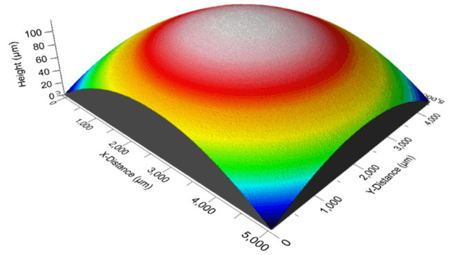
The New ERM Benefits Several Different Applications
The new ERM is designed to significantly improve optical measurements in the following areas:
- Lenses, such as Fresnel lenses, due to the ability to measure steeper slopes. The Profilm3D can now measure lenses for up to 60° of slope using a 50X lens, with >50 percent measurable pixels
- Very rough surfaces on chemical mechanical polishing (CMP) pads
- Biomedical implants
- Precision machining
- Semiconductor wafer applications, such as ball grid array (BGA) and stepper aspect ratio vias
- Semiconductor IC packaging applications, such as probe marks, wire bond imprints and lead frame roughness
- Automotive applications such as brake pad roughness and cylinder roughness
- Solar device manufacturing (details below)
Benefits of ERM in Solar Device Manufacturing
Solar devices use photovoltaic technology that absorb incoming sunlight to convert to electrical energy. This is typically done by including aluminum (Al) to enhance conductivity, as it is resistant to oxidation in outdoor environments. The solar cells are also typically coated with a silicon (Si) or gallium arsenide (GaAs) substrate, which helps reduce its surface reflectivity. For optimum performance of a solar device, one needs to closely monitor the dimensions of the deposited Al lines as well as the surface roughness of the substrate (Si or GaAs) to ensure uniformity.
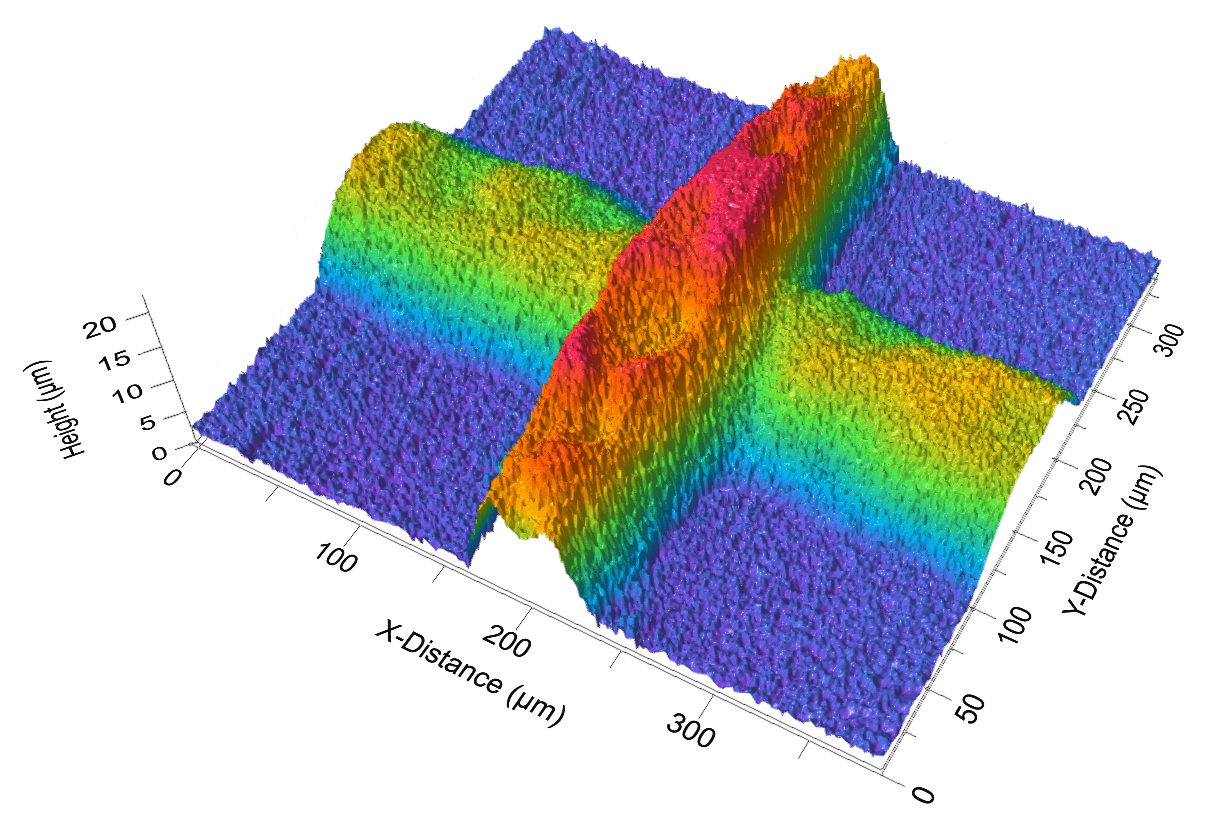
Rapid measurement of both surface roughness and critical dimension are possible with the newest Filmetrics® Profilm3D which combines key technological advances to enable measurement of even the most challenging optical elements on a solar device. Using ERM, the Profilm3D captures a higher fraction of the low reflectivity and rough texture signals without saturating the optical detector. This approach provides a more accurate measurement of both the textured surface and the dimensional variation of the metallization lines. Multiple adjacent images of the solar cell area are easily combined into a single large-area measurement that can be quickly analyzed, showcasing the power and flexibility of the optical profiler for process monitoring, characterization and R&D.
TotalFocus™ Infinite Depth-of-Field Imaging
With a traditional microscope, it is impossible to simultaneously focus each pixel across the entire field of view. The new Profilm3D’s TotalFocus™ mode utilizes the 3D measurement data of a surface to produce an image with every pixel in focus, resulting in crisp, clear high-magnification images.
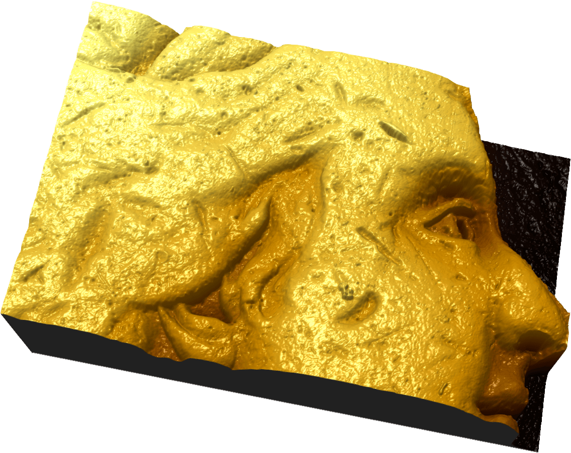
Benefits of TotalFocus™ Imaging in MEMS, Micromachining and 3D Printing
MEMS, micromachining and 3D printing applications commonly feature large variations in the Z plane and often require measurements larger than a single field of view, especially at higher magnifications. They may also have combinations of material reflectivity or unusual surface contours that are challenging to measure with a single experiment recipe. Instead of having to use multiple scans or tools, the Profilm3D uses a simultaneous measurement technique that combines the detail of TotalFocus™ with the speed of interferometry to produce a single 3D measurement image. This technique is robust enough to measure various parameters including low reflectivity, high slope, rough, and large step samples, thus providing the ideal measurement method that is best suited to any given sample type.
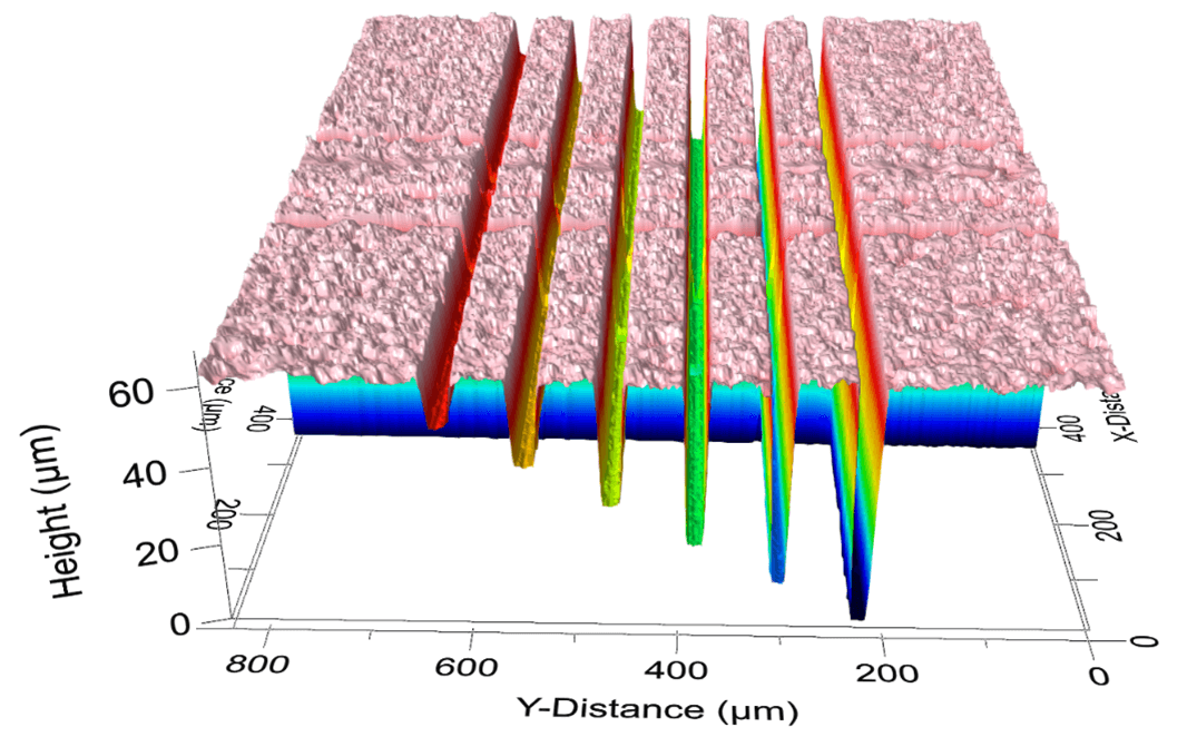
Profilm3D Advantages
KLA Instruments optical profilers serve several different industries, including compound semiconductors, data storage, solar and display, biomedical and pharmaceutical, automotive, and aerospace, metal/glass/ceramics manufacturing, academic research and more. The Profilm3D provides several advantages over its competitors:
- High quality measurement data at an affordable price point
- Powerful tool capabilities that can be used by development engineers in both production and QA environments
- 500µm Z piezo travel for measurement of features that are taller than a typical scan range, thus removing the need for multiple scans or lower resolution stages to stitch the images together
- Easy collaboration: KLA Instruments™ differentiates the Profilm3D by including a collaborative online data viewing and analysis platform
- ProfilmOnline supports sharing data with your colleagues using either a public or private database and has all the analysis features that come with the Profilm3D optical profiler, but with cloud-based analysis that can be accessed through any browser
Where can I learn more?
KLA Instruments is exhibiting at Booth 2066, Photonics West, January 25-27, 2022. The new Profilm3D tool will be on display for live demos. You can also contact us here to learn about additional capabilities on the Profilm3D such as True Color Imaging and Phase Shift Imaging that are available for your individual needs.
Follow Us