This Earth Day, we commend the efforts of our customers and partners throughout the electronics ecosystem who continue to find ways to reduce their environmental impact. Within the semiconductor segment, companies are focused on reducing their environmental footprint through a range of initiatives including water recycling, renewable energy use, reduced emissions and efficient building design. In addition, chip manufacturers employ continuous improvement programs to optimize their operations and work with their supply chain to directly reduce the resources used in fabs.
Background
To produce chips, semiconductor fabs start with silicon wafers and precisely add and subtract specialized materials, creating nanoscale patterns that form the transistors and connectors that determine the chips’ functions. It can take four to six weeks from the time a wafer enters a fab until processing is complete, during which time it may pass through a thousand process steps. Each step involves process tools and materials that must meet rigorous quality standards to ensure that the resulting chips are functional, reliable, and meet power and performance specifications. If something goes wrong at a single process step, it can cause lower performance, functional inconsistencies or outright failure of the chips. Chips that do not meet quality standards are scrapped.
Because chip manufacturing requires energy, wafers, chemicals and other resources, from an environmental perspective, it’s imperative to ensure that all process steps meet stringent quality standards to prevent wafer scrap and reduce wafer rework. That’s where process control comes in – inspection and metrology systems measure the wafers after process steps and look for problematic defects or variations that can cause chip performance, reliability or other quality issues. Identifying process issues early allows fabs to take quick corrective action, reducing scrap and rework – and ultimately, reducing resource consumption.
Fabs looking for creative ways to further reduce environmental impact are upgrading their process control solutions to be more capable and adding additional inspection and metrology steps. These process control green schemes reduce scrap and net resource consumption per good die out.
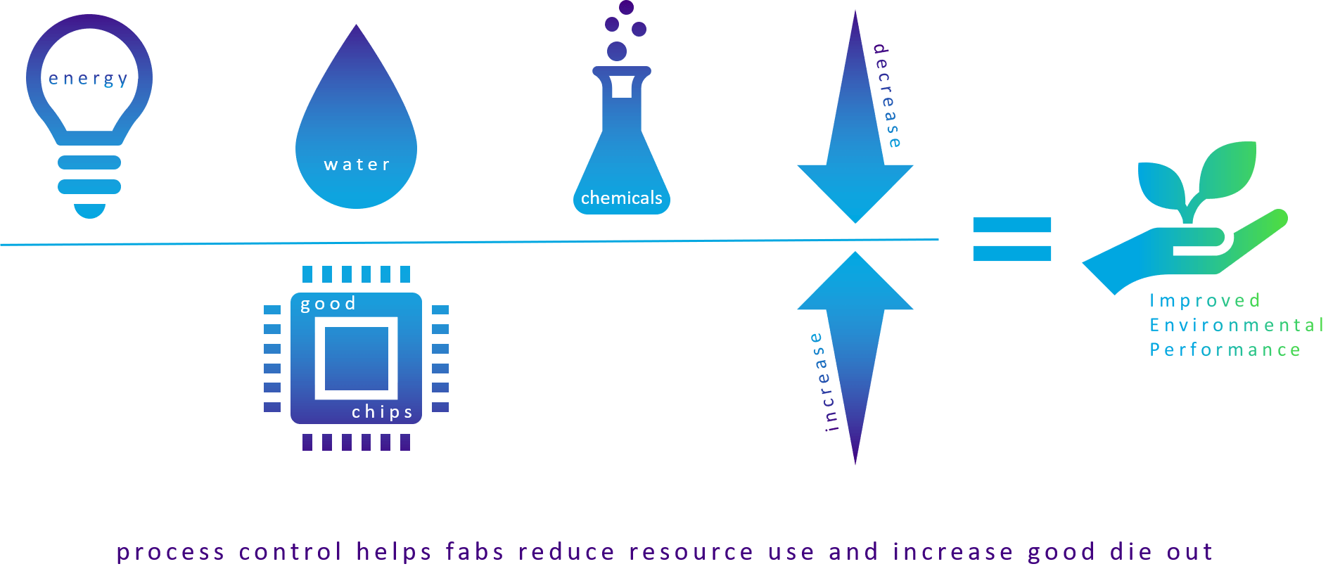
Green Scheme 1: Improved Process Control Performance
Process control provides the data necessary for fab engineers to make production wafer dispositioning decisions and to address process issues. For example, if after-develop inspection (ADI) data indicate a high number of bridging defects on patterned wafers following a particular lithography patterning step, the lithography engineer takes several corrective actions. In addition to sending the affected wafers back through the litho cell for rework, the engineer will stop production through the litho cell to fix the underlying process issue. These actions limit the amount of material impacted and potentially scrapped.
To be effective, however, the quality of the process control measurement is critical. If an inspection or metrology tool has a lower capture rate or higher total measurement uncertainty (TMU), it can erroneously flag a process excursion, sending wafers for unnecessary rework, causing additional consumption of energy and chemicals, and production of additional waste. Alternatively, if the measurement fails to identify a true process excursion, the yield of the product is negatively impacted and more dies are scrapped—again, resulting in less desirable environmental performance.
The example shown examines the environmental impact of data produced by two different metrology systems in the lithography cell. Implementing metrology system B, with better measurement performance, improves the quality of the process control data, enabling the lithography engineers to make better process decisions.

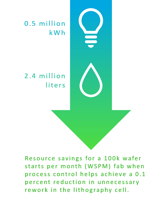
Implementing a better performing metrology system results in power and water savings, plus a proportional percentage reduction in the amount of resist and clean chemicals consumed.
Green Scheme 2: Earlier Excursion Detection
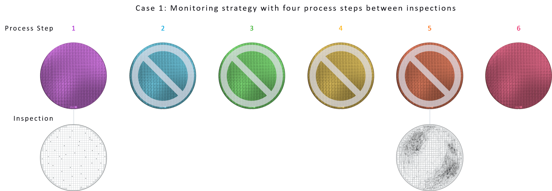
Fabs are also reducing process excursions by adding inspection and metrology steps. This example shows two methods of deploying an inspector in a production fab. In the first case, inspection points are set such that a lot is inspected at the beginning and end of a module, with four process steps in between. If a process excursion that results in yield loss occurs immediately after the first inspection, the wafers will undergo multiple processing steps, and many lots will be mis-processed before the excursion is detected.
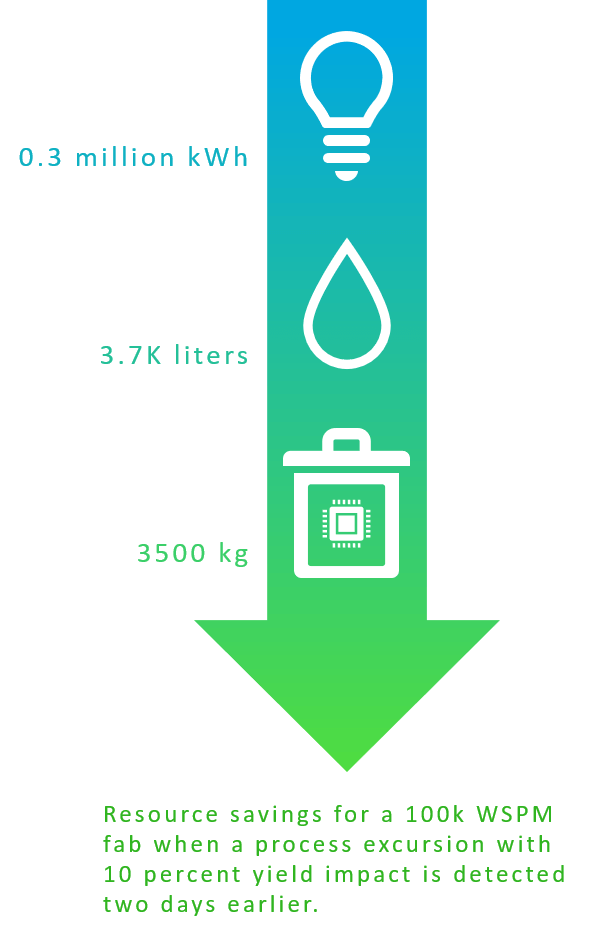
In the second case, inspection points are set with just two process steps in between. The process excursion occurring after the first inspection point is detected two days sooner, resulting in much faster time-to-corrective action and significantly less yield loss and material wasted.
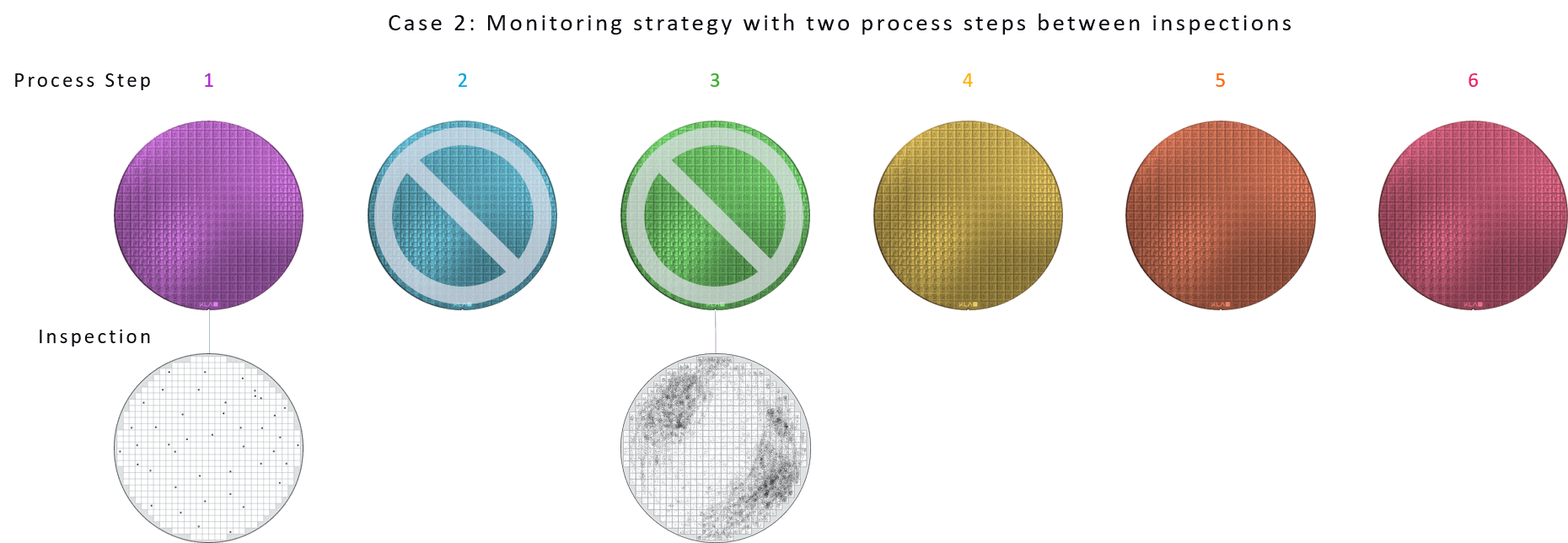
This two-day difference in detection of a process excursion reduces waste and provides a significant resource savings. While these environmental benefits were obtained by sampling more process steps, earlier excursion detection and improved environmental performance can also be obtained by sampling more sites on the wafer, sampling more wafers per lot or sampling more lots. When a careful analysis of the risks and associated costs of yield loss is balanced with the costs of additional sampling, an optimal sampling strategy has been attained.
Conclusion
As semiconductor manufacturers focus more on their environmental performance, yield management serves as a critical tool to help reduce a fab’s environmental impact. Fabs can obtain several environmental benefits by implementing higher quality inspection and metrology systems, optimal process control sampling and faster cycles of learning. A comprehensive process control solution not only helps chip manufacturers improve yield, but also reduces scrap and rework, reducing the fab’s overall impact on the environment.
Follow Us