Part II of this series on integrated circuit (IC) substrates focuses on six yield-critical challenges ICS manufacturers should tackle to enhance their competitiveness, drive higher yield rates and position themselves as leaders in the semiconductor industry.
Three key trends are currently impacting the yield of advanced IC substates: first, IC substrates (ICS) are getting thicker, with more and more layers; second, the substrates are getting larger to support more complicated packaging integrations; and third, the dimensions are reducing on features like the lines and spaces.
As ICS feature complexity grows, achieving desirable high yield and reliability depends heavily on the ability to solve process and process control challenges. Manufacturers can minimize defects and improve overall yield rates by continually refining their processes. Implementing process control is crucial for identifying and eliminating defects at various steps of production.
Six Key Process Challenges
Unique and Expensive Materials
Maintaining Film Quality for ABF
Reducing Void Defects
Drilling Tiny Vias in the Right Place
Patterning the Finest Lines
Copper-on-Copper Defectivity
Read part I of this series to learn about trends in the electronics industry making IC substrates a key element for semiconductor packaging and a new frontier for innovation.

To illustrate a typical example of the kind of intricate processing and the problem-solving required, let’s take a closer look at a typical example of an ICS process flow. Manufacturing an IC substrate with a core using an ABF (Ajinomoto Build-Up Film®) high-end, semi-additive process (SAP) starts with a design phase and pre-manufacturing optimization and then is followed by an iterative process of creating interconnections between the core and the next layer (steps 1-5 below) and then building the connectors between every layer to the next (steps 6-10). Each of the 10 process steps following the pre-manufacturing optimization introduces new process challenges. In this article, we’ll focus on the six hardest challenges.
ICS yield optimization can start even before manufacturing begins, with what we can call step 0.
0. CAM (Computer-Aided Manufacturing) and Engineering
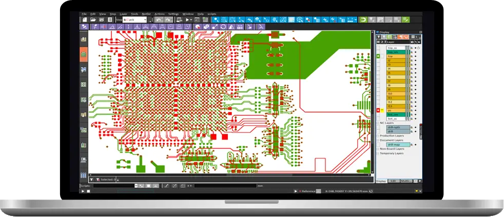
Pre-manufacturing steps can boost yield significantly. Those steps involve using software to generate the instructions for the tools that will be used to manufacture IC substrates. CAM and engineering software take design data and optimize it to cope with process capabilities and generate the necessary tool data and parameters, which can include drilling, routing, imaging, inspection and other operations.
ICS Process Challenge
Unique and Expensive Materials
To avoid waste and optimize efficiency, workflows for all job types can be automated. Manufacturers can benefit from automatic analysis, optimization and panelization to fully utilize materials, making manufacturing processes more efficient.
1. Preparation of the Substrate Core
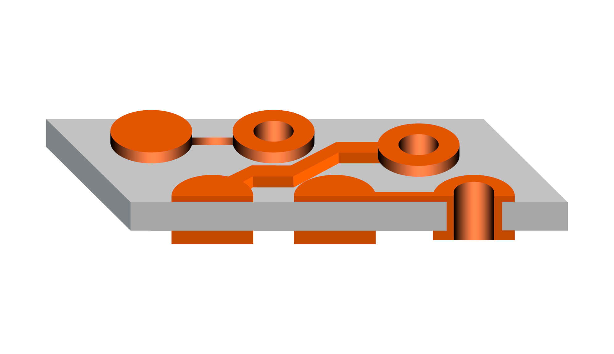
The core layer of an IC substrate is made of a rigid material, such as epoxy resin or fiberglass-reinforced laminate, on top of which multiple layers of insulating materials and conductive traces made of copper are built, using a sequential buildup process. For proper addition of the ABF and subsequent line structures, the ICS core will serve as the foundation for buildup circuitry.
2. Building Circuitry with ABF Base Material to the Core
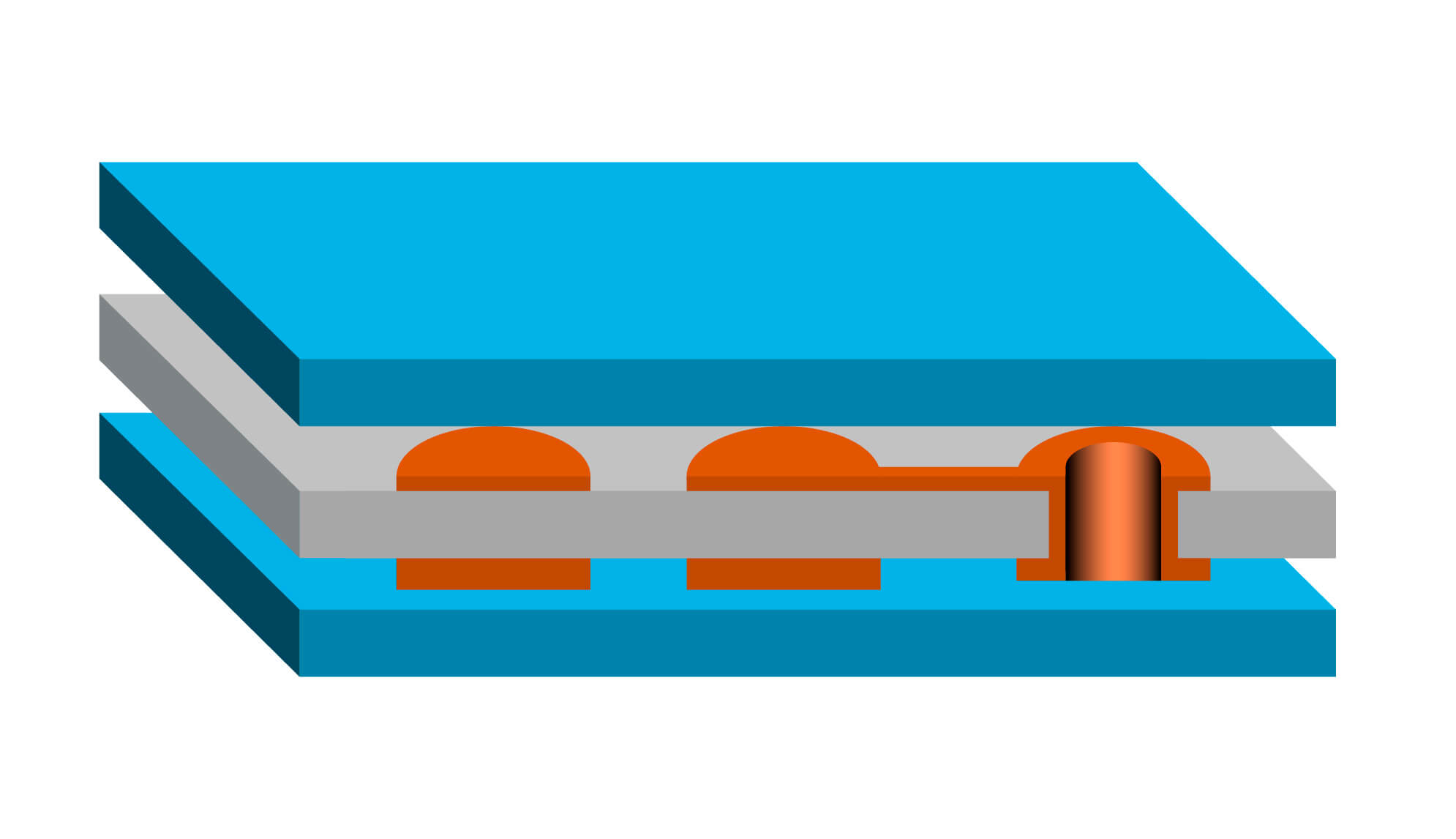
ABF is used as an insulating material on the ICS for ultimately protecting high-performance semiconductors inside packages. It has low surface roughness and enables the coating of very thin copper down to 1 µm, which can be served as a seed layer for future circuitry buildup.
The ABF-coated ICS core is then placed in a vacuum lamination machine, using heat and pressure to bond the ABF film to the ICS core securely. The vacuum environment delivers proper adhesion by removing air bubbles and contaminants.
Once the ABF is laminated onto the ICS core, a metal hot press is applied. PET foil, a high-density polyester, is placed on top of the ABF layers on both sides of the core. The assembly is then subjected to high temperature and pressure, causing the ABF to bond with the copper.
ICS Process Challenge
Maintaining Film Quality for ABF
A key process challenge during ABF lamination is maintaining a uniform film thickness. Variations in the ABF thickness can result in non-uniform electrical performance and lower circuit reliability. Metrology systems are crucial for monitoring this thickness. A precise measurement allows for better tuning of via drilling; see process step No. 4. As packages evolve toward more layers and finer line spaces, the ABF thickness will soon reach 10 µm. This trend will also have implications for the metrology requirements.
3. Pre-Curing for Structural Reinforcement
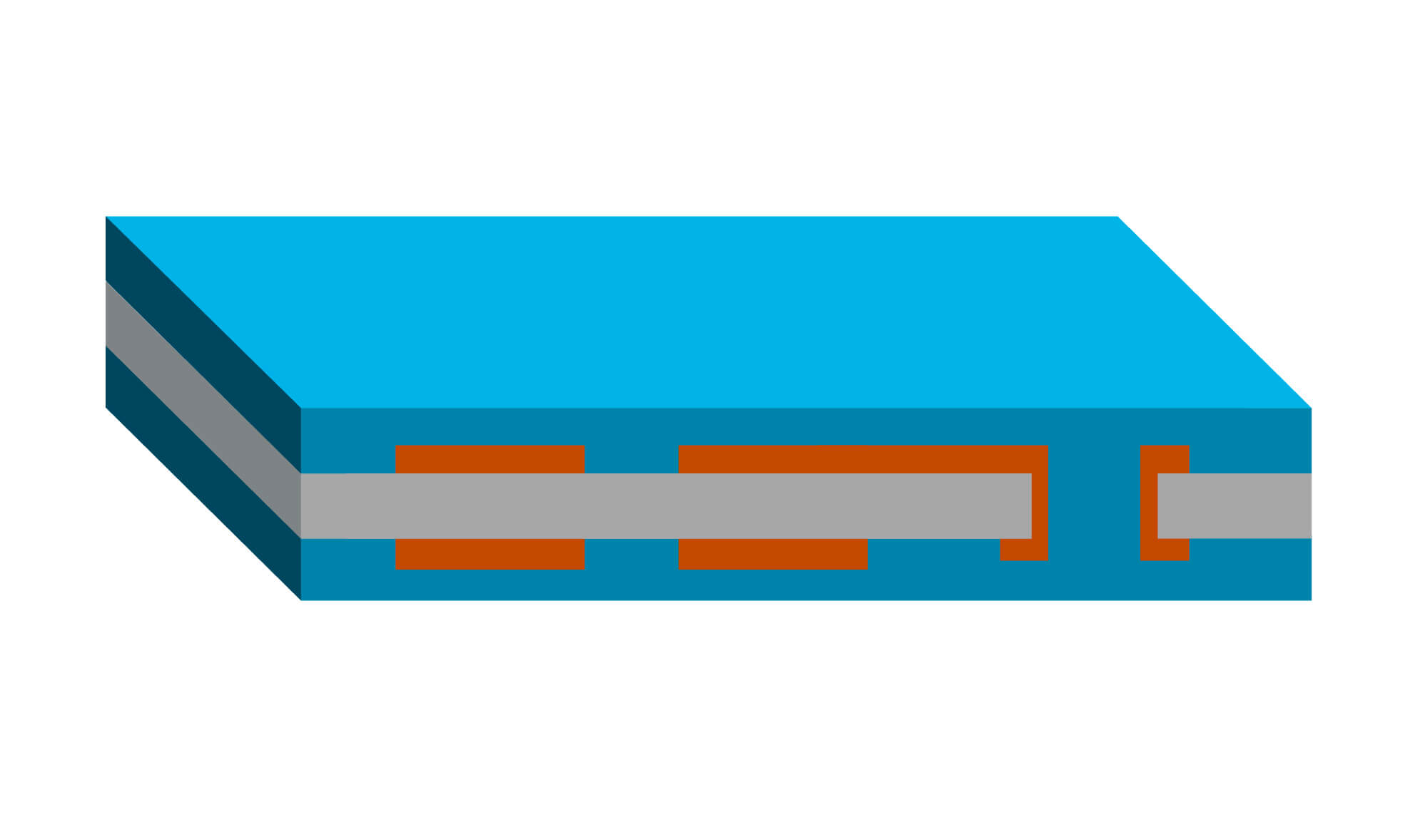
Pre-curing bonds the layers properly, resulting in a structurally stable substrate. During the pre-cure phase, the IC substrate undergoes a hot air clean-over process to remove any excess debris, impurities or residue that may have accumulated during the previous steps. The substrate is exposed to a stream of high-temperature air to help evaporate any remaining solvents or volatile materials from the substrate and remove particles or contaminants by blowing them away.
The hot air clean-over is performed in a controlled environment, such as a cleanroom, to minimize the introduction of additional particles or impurities. This step is crucial to maintaining the substrate’s electrical performance and reliability.
ICS Process Challenge
Reducing Void Defects
Voids — the empty spaces or air gaps that may be present within the substrate material — can cause various issues in IC substrates, such as reduced electrical performance, thermal dissipation problems and mechanical integrity concerns. This may result in the creation of “shorts” (unwanted electrical connections) between the layers in the next processing stage.
Inspecting the thinner substrates to detect voids after the pre-cure phase is crucial for maintaining the quality and reliability of the IC substrate. Several challenges for defect inspection must be overcome to establish an effective process control strategy to find and reduce void defects quickly.
Smaller yield-critical defects: The critical size of voids that could impact the yield of the substrate continues to get smaller, especially in advanced manufacturing processes. Detection of these minuscule voids requires extreme high-resolution inspection and advanced image-acquisition capabilities.
Size and shape variability: Voids can occur in different sizes, shapes and depths, ranging from microscopic to macroscopic dimensions. The irregular shapes and varying sizes embedded inside the laminate make it challenging to establish a uniform inspection process that can accurately detect voids.
Substrate complexity: IC substrates often have complex multilayer structures with different materials and patterns. These complexities can create shadows, reflections or other optical distortions that make it difficult to differentiate accurately between voids and other features like silica filler found in ABF.
Substrate surface roughness: Irregularities or roughness in substrate surfaces make it challenging to distinguish between voids and surface imperfections. Finding 3D defects with a 2D inspection machine is challenging. The inspection system must be capable of identifying and discriminating true voids from surface anomalies.
Need for speed: Because high-production throughput is essential in IC substrate manufacturing, the inspection process must be performed rapidly. Ensuring efficient and accurate void inspection within the required time frame poses a significant challenge.
Accurate defect sorting: The inspection system must strike a balance between minimizing false positives (detecting voids that are not present) and false negatives (missing actual voids). It requires high-sensitivity optics paired with advanced algorithms to identify voids accurately and minimize the chances of misinterpretation.
Data interpretation and analysis: The inspection process generates a vast amount of data, including images, measurements and statistical information. Effectively analyzing and interpreting this data to identify voids and assess their impact on the substrate’s quality can be a complex task.
To address each of these challenges, manufacturers must employ advanced inspection techniques using the most advanced automated optical inspection (AOI) systems. These technologies are designed to improve void detection accuracy and increase the overall quality and yield of IC substrate manufacturing. Advanced root-cause analysis can be realized by combining the inspection data with analysis based on CAM outputs to deliver improved yield control and production efficiency.
4. Via Formation
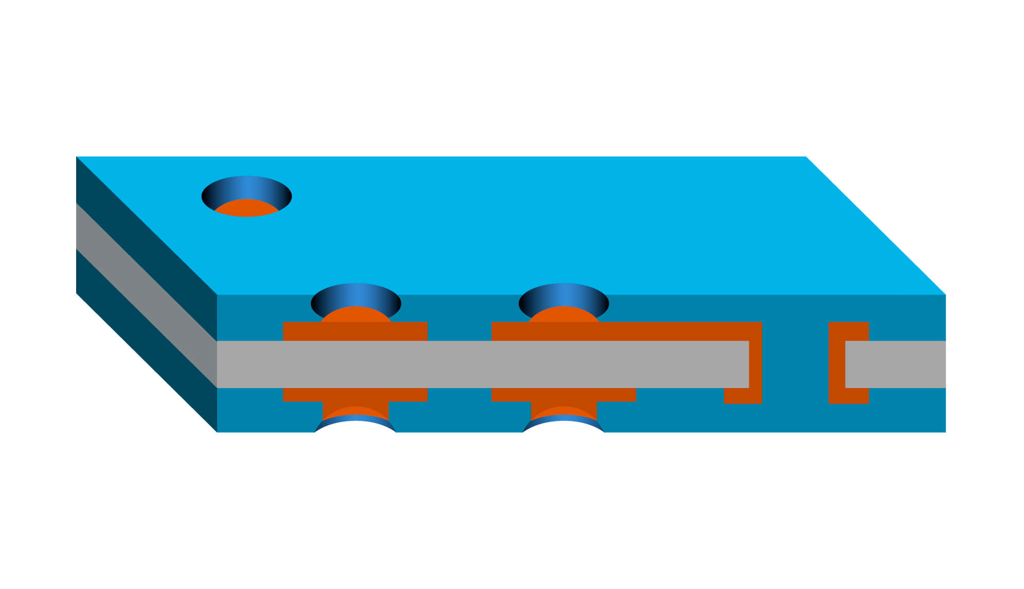
Forming vias — small holes or openings that can be plated for electrical signals to pass through the substrate layers — is a crucial step in creating interconnections between different layers of the substrate. Two current drilling techniques for IC substrates include the use of lasers — CO2 ablation and UV laser drilling. For higher accuracy and improved operational aspects, patterning of photo-imageable dielectric (PID) material using an extra thin dielectric layer is expected to be adopted. However, for this discussion, we will focus on the laser methods.
CO2 Laser Ablation: The Cost-Effective Option
Organic substrates, ceramic material and certain polymers can be ablated with CO2 lasers using a high-powered laser-emitting light with a wavelength that is absorbed by the material. The laser’s energy is converted into heat, causing localized vaporization and ablation of the material.
CO2 lasers can drill directly on ABF and other IC substrates, forming rounded vias with acceptable tapers (top of the via is larger than the bottom). The copper or metal pads do not absorb CO2 light and thus act as a stopping layer, preventing damage to the pad. This is different from UV lasers, where copper absorbs almost all UV light radiation. Therefore, it is possible to damage or burn through the copper pads with UV lasers.
In general, CO2 lasers are more powerful and cheaper than UV lasers. This allows CO2 machines to drill faster than the UV systems typically employed in the IC packaging industry. Furthermore, the CO2 lasers are easier to maintain in terms of optical integrity, reducing the need for maintenance and spare optical parts. This, in turn, lowers their running costs.
However, CO2 lasers typically have larger beam spot sizes compared to UV, resulting in larger via diameters and limited resolution. Due to their wavelength and ability to absorb into various materials, such as conductive copper layers, CO2 lasers, while versatile, are still limited in beam size.
UV Laser Drilling: Smaller Vias
UV lasers traditionally employ a 355 nm ultraviolet laser beam which can ablate various materials due to the high absorption of such light. Using UV lasers, metal layers like copper, aluminum and gold can be drilled easily. Furthermore, UV systems easily ablate organic and non-organic substrates like ABF, polymers and epoxies. This combination of conductive and non-conductive layer drilling is most suitable for the flex PCB market where drilling through copper layers is required.
Due to their short wavelength of light, the beam sizes can be much smaller, allowing for the drilling of smaller features than that of CO2 lasers. With UV lasers, small vias can be drilled directly into substrates such as ABF in the ICS market, which cannot be done with CO2 drilling.
UV lasers are generally less powerful than CO2 lasers. A CO2 laser has an output of 80+ watts and costs less than its UV equivalent, which has an output of 20-30 watts. In addition, UV systems require special coatings on optical components, which degrade over time, thereby increasing factory maintenance and operating costs.
In the ICS ABF drilling market for flip chip BGA packaging applications, both CO2 and UV systems have their advantages and disadvantages. For advanced applications, UV systems can drill much smaller vias than the CO2 equivalent (under 40 µm). UV laser systems do not require a sacrificial PET layer for drilling. The PET layer that was used for applying the ABF onto the panel is removed prior to UV drilling, otherwise the PET layer expands thermally when the UV laser is applied and bonds to the ABF. This, in turn, deforms the via, causes burn marks and affects the minimum pitch between the vias.
In CO2 drilling, the beam sizes are limited due to the wavelength of light, making it difficult to drill features smaller than 40 µm. CO2 lasers can drill with or without the sacrificial PET layer. For vias smaller than 60 µm, the sacrificial PET layer is used to make the vias on the ABF smaller without shrinking the beam size. Due to thermal expansion from laser drilling, the top of the via is always larger than the bottom of the via, which is called a “taper.” If the beam must travel through the PET layer first, the via or hole in the ABF is much smaller than the hole in the PET layer, enabling the drilling of smaller vias, but CO2 laser drilling machines are traditionally limited to vias larger than 40 µm.
ICS Process Challenge
Drilling Tiny Vias in the Right Place
IC substrates are becoming increasingly compact and complex, with smaller feature sizes and higher circuit densities. As features become smaller and more features are present on each layer, both accuracy and throughput play a critical role in the production process.
Since UV systems can drill smaller features, they may be more suitable for entering the advanced ICS market. However, as most ICS via sizes are still above the 40 µm-diameter range, CO2 lasers are a sensible choice due to their lower costs and faster throughput.
Challenges still arise for the laser drilling process, especially with the transition to smaller pads to save real estate and the need for more cost-effective manufacturing. The challenge of fast and accurate target acquisition in IC substrate laser via drilling arises from the need to locate the target area quickly and accurately on the substrate and initiate the drilling process so that all vias land on the pad without affecting adjacent circuitry.
Several factors contribute to the complexity of this high-accuracy task:
Alignment accuracy: The laser drilling system must be able to align the drilling beam with the target location accurately. Misalignment, even by a small margin, can result in damage to neighboring circuit elements. Achieving sub-micron level alignment accuracy is essential for laser drilling to take place in the correct location.
Substrate variations: IC substrates come in various materials, thicknesses and surface finishes, each with its own unique characteristics. Variations in laser drilling processes can complicate the development of a universal target acquisition solution. The system must account for such variations and adapt accordingly.
Real-time feedback: Fast target acquisition requires real-time feedback to provide precise positioning and drilling. Sensors, vision systems or other monitoring techniques can deliver this feedback. Integrating such feedback mechanisms into the drilling process and effectively interpreting the data pose additional challenges.
To address each of these challenges, laser drilling solutions combine precise positioning techniques, real-time feedback and intelligent algorithms to optimize the target acquisition process and improve overall efficiency.
To reduce costs, throughput must also be improved.
Need for speed: In modern manufacturing environments, achieving the throughput required for high volume is essential to maintain competitiveness in the market and drive costs down. The challenge of increasing throughput requires innovative system approaches for beam delivery to the panel. Advances in lasers, electro-mechanical devices and optical delivery systems are crucial for improving drilling throughput.
5. Micro-Etching and Adding a Copper Seed Layer
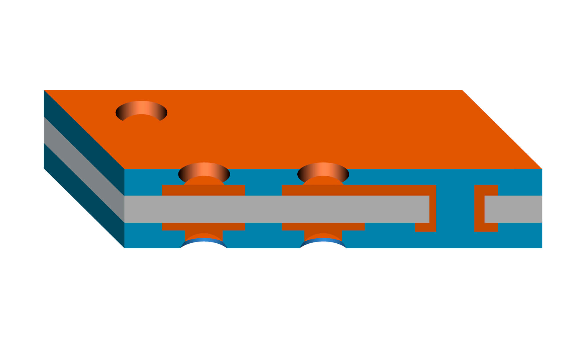
This step starts with micro-etching, the highly selective removal of material to increase surface area inside vias for better copper-to-ABF adhesion. Then, on the clean surface, electroless copper plating is first used to deposit a thin layer of copper, followed by a drying step to prepare the substrate for further processing. These steps are crucial for achieving a clean, conductive surface that can support the fabrication of integrated circuits with reliable electrical connections.
The next phase (steps 6-10) involves creating the conductors through a photolithography process.
6. Photoresist Coating
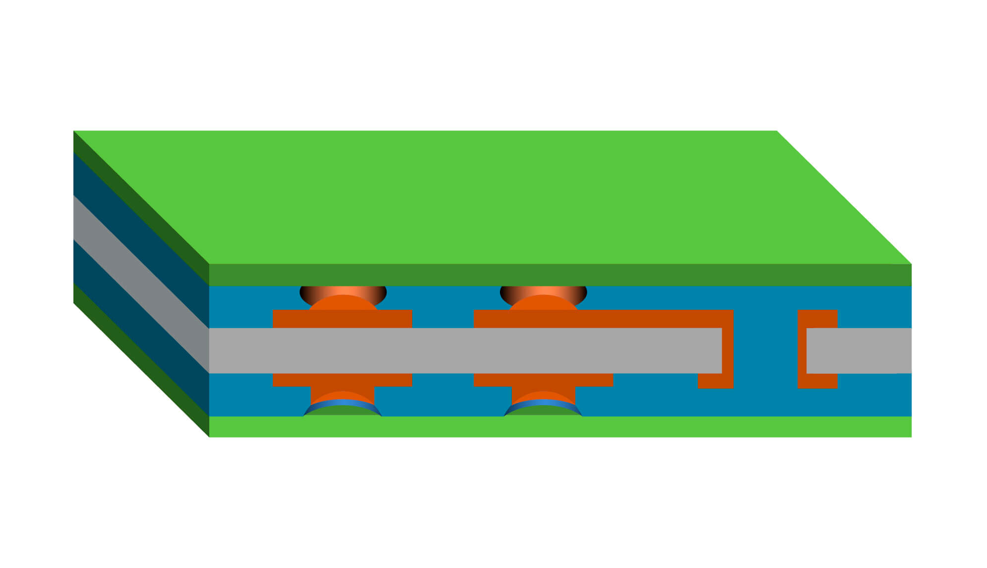
The most popular photoresist coating is a layer of dry film, which is applied by lamination to the surface of the substrate. For optimized performance, manufacturers may use a liquid resist applied through a deep or spray-coating technique. Once copper patterning is done creating the circuit patterns and interconnections on the substrate, the photoresist coating will be removed (step 9).
7. Creating the Circuit Patterns
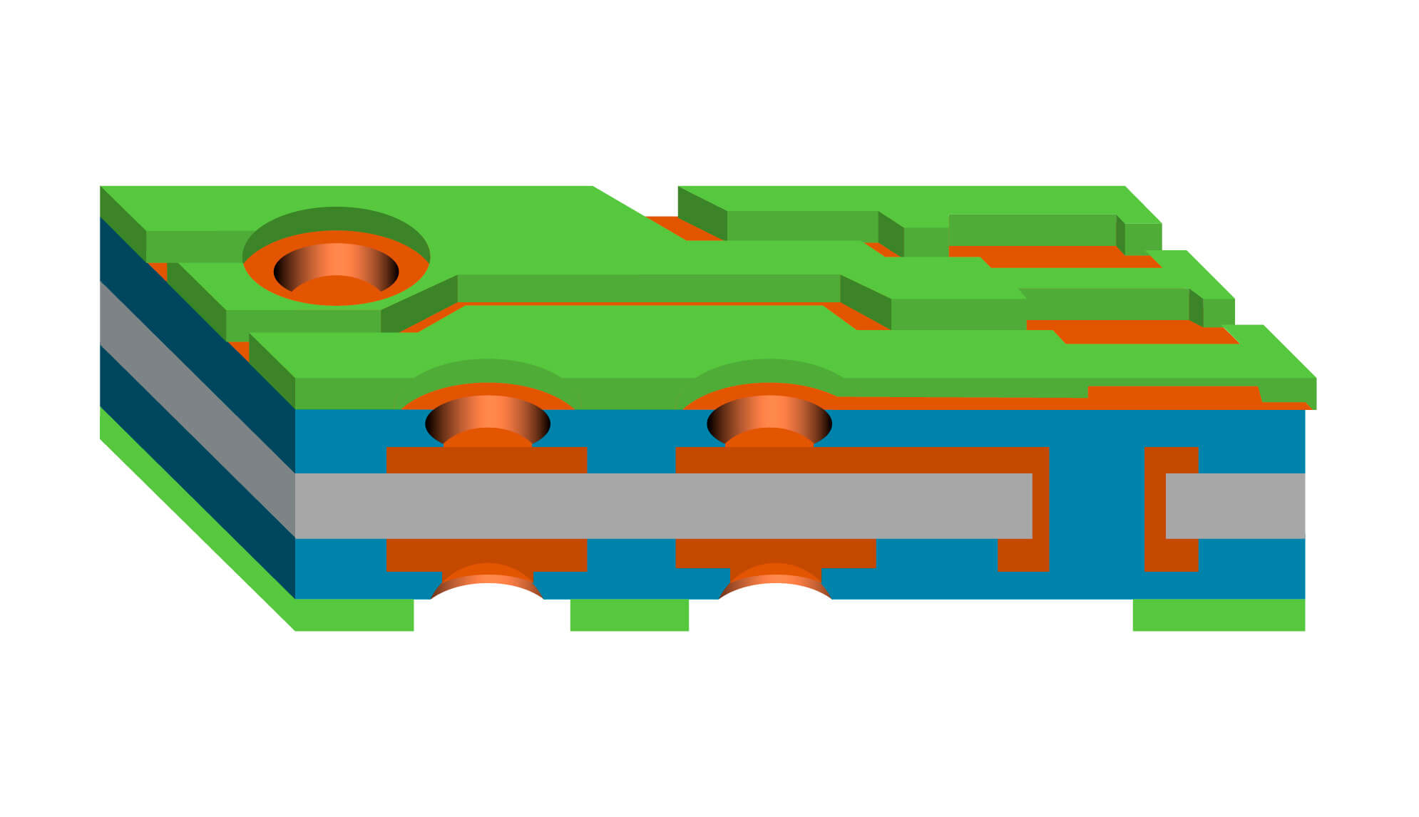
The image transfer (also known as photolithography) performed on laminated photoresists that are on the substrate surface plays a crucial role in defining the circuit patterns on IC substrates. It enables the creation of intricate and precise connections required for electronic devices. The accuracy and quality of this step directly impact the performance and reliability of the final product.
Image transfer can be done either through direct imaging (DI) or conventional solutions such as steppers and contact exposure tools. Existing mainstream ICS typically use direct imaging, whereas more advanced IC substrates rely on steppers.
Steppers use a projection lens to create a pattern on the photoresist. Through a step-and-repeat process, the pattern is transferred onto the photoresist one portion (or “step”) at a time. This process is repeated until the entire pattern is exposed onto the substrate. Steppers use photomasks, which contain the pattern, and they project the pattern onto the substrate using a light source, such as an ultraviolet (UV) lamp.
DI systems, on the other hand, use laser beams or UV lamps to transfer patterns directly to the photoresist. This makes them advantageous for faster time to market, and cost saving, as they eliminate the need for expensive photomasks and associated operation costs.
ICS Process Challenge
Patterning the Finest Lines on Uneven Surface Topography
Today, the requirement on IC substrate manufacturers to pattern extremely thin conductors and transmission lines calls for extreme registration and overlay accuracy. These copper traces must be formed with extreme precision, as circuit density increases and the distance between lines narrows.
This is no easy feat, given the inherent challenges of creating these complex circuits on different substrates, all while keeping high quality at a competitive cost per print. Here are some of the main challenges associated with step 7:
Overcoming the Accuracy-Versus-Speed Tradeoff
Advanced IC substrate patterning requires high overlay accuracy, which can be achieved by using more substrate partitions and patterning targets. However, this mode of operation impacts system throughput as it requires more time to read and process a larger number of targets. Usually, an increased number of targets will result in a lower throughput.

Achieving High Imaging Quality
ICS circuit designs consist of intricate patterns and structures that continue to get finer to provide increasingly dense circuitry with increased performance. A common measure of the feature sizes on the substrate is the pitch, which is defined as the width of line and the adjacent space. A smaller pitch value indicates a higher density of lines and spaces.
The importance of the exposure focus (i.e., depth-of-focus, autofocus) mechanism increases as pitch narrows and surface topographies become more complex because of new challenges like surface distortions that must be overcome.
In the context of photolithography, depth-of-focus (DOF) can be thought of as the range of focus that keeps the resist exposure profile of a given feature within all production specifications. A higher depth of focus means a larger range of focal points can be applied during the exposure process, which can increase the exposure quality and offer a larger production working window.
Advanced IC substrates pose a double process challenge, combining nonuniform surface topography with a very small pitch value. A low depth of focus is not fit for purpose. A large and continuous focus mechanism delivers better imaging quality.
8. Copper Electroplating
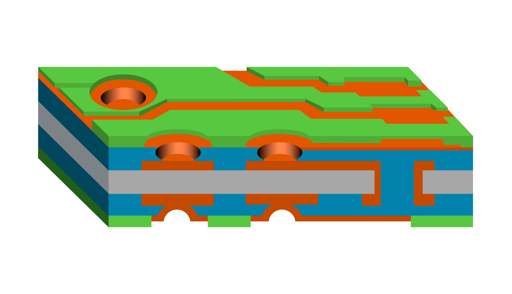
The goal of the copper electroplating stage is to deposit a layer of copper onto the patterned substrate surface and achieve a uniform and controlled growth of the copper layer for optimal performance.
During the electroplating step, the substrate is immersed in a plating bath containing a solution of copper ions. The plating bath consists of copper salt and other chemicals to control the plating process.
Copper is an excellent conductor of electricity, and the electroplating process allows the formation of a uniform layer of copper traces and interconnects on the substrate. These copper traces act as conductive paths for the electrical signals within the substrate. As soon as the conductors reach the desired dimensions, the photoresist film may be removed.
9. Removal of the Photoresist Film by SAP (Semi-Additive Process)
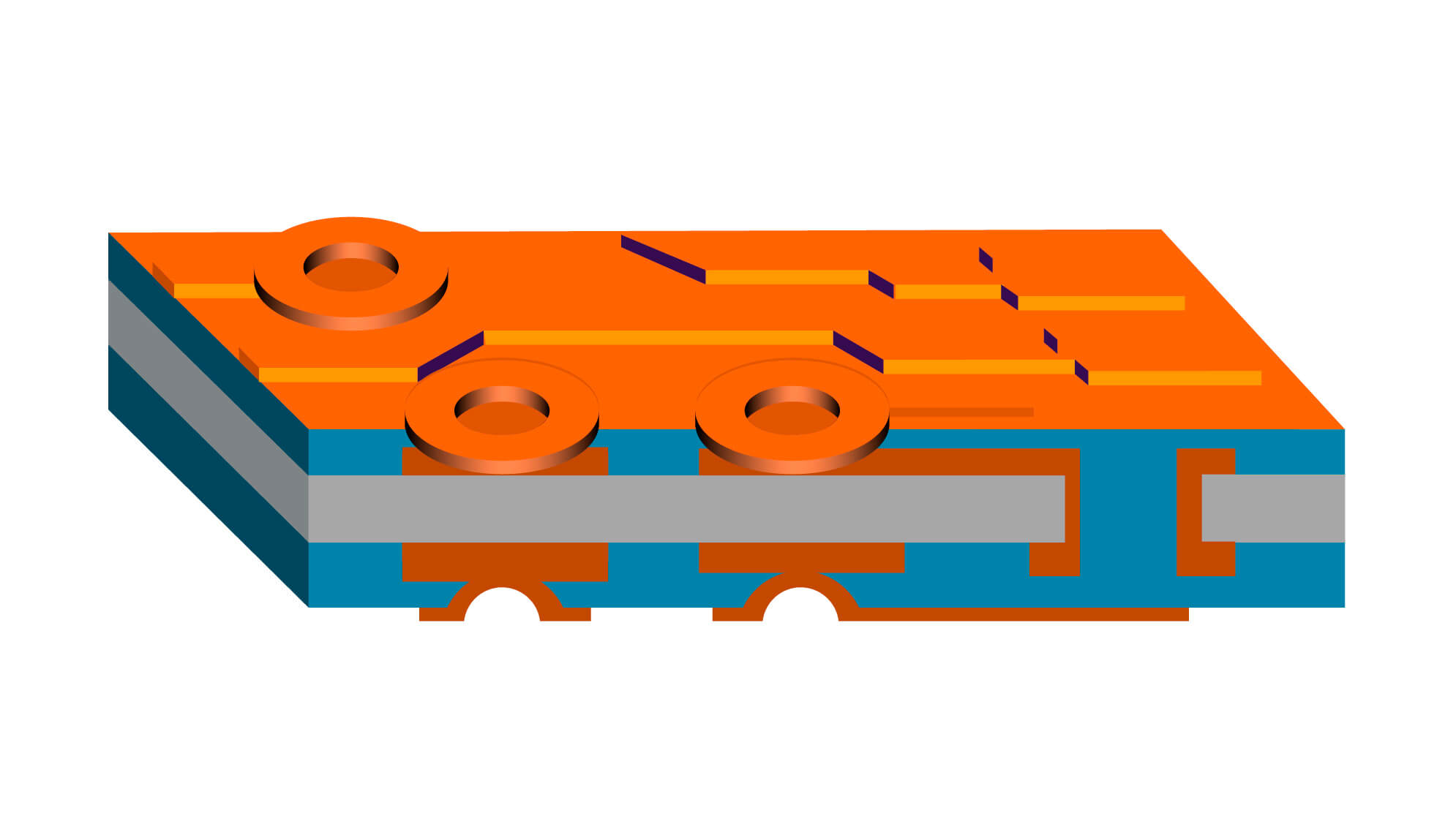
The dry film resist (DFR) acts as a temporary protective layer during the plating process. Once the copper electrodeposition is complete, the remaining dry film resist needs to be removed to reveal the copper circuitry. Prior to removal, the DFR is softened by exposing it to an appropriate solvent or chemical solution, making it easier to remove.
The softened DFR is mechanically agitated, either through brushing, scrubbing or using high-pressure water jets. This physical action helps to dislodge and remove the softened DFR from the substrate’s surface. After the mechanical removal of the DFR, the substrate is rinsed thoroughly with deionized water or a cleaning solution to remove any remaining DFR residue or contaminants. Finally, the substrate is dried by air drying or a combination of forced air and heat.
After the dry film resist removal, the exposed copper circuitry must undergo additional etching and surface treatment to refine the circuitry or enhance its performance.
ICS Process Challenge
Copper-on-Copper Defectivity
While common IC substrates use an ABF laminate seed layer, advanced ICS, such as those used in FC-CSP (ETS process) use a copper base (seed). The term copper-on-copper inspection refers to inspecting a copper pattern above the copper base (seed) layer, with the aim of detecting pattern defects such as shorts (unwanted electrical connections), nicks, opens and dish downs (dent depressions on the copper surface), etc.
Copper-on-copper inspection presents two main challenges:
Detection of fine defects on the upper copper surface: Lack of contrast in the absence of organic materials like ABF complicates image acquisition. High sensitivity for fine copper defects will result in a high defect count. While defects on the upper copper layer are critical, those on the seed layer are negligible. The main challenge is distinguishing between the two.
Fast and accurate differentiation between real and false defects: Differentiating between critical and negligible (not yield-impacting) defects on the seed layer as a result of missing copper is difficult. For example, dust or oxidized areas can easily be mistaken for a real defects but in fact, can be cleaned. The inspection system should be able to differentiate between oxidized areas and more critical, yield-impacting defects of interest.
The way to handle these challenges is by using automated optical inspection (AOI) systems equipped with advanced image acquisition technology. Multi-imaging is a technology that applies a customized recipe that integrates images from different angles, wavelengths, light intensity and other factors into a single multicolor image. The next step, image processing, requires advanced algorithms to handle the multi-image that enables ICS manufacturers to distinguish between the upper copper and the seed layer and therefore between real and false defects.
10. Finalizing the Circuit Patterns
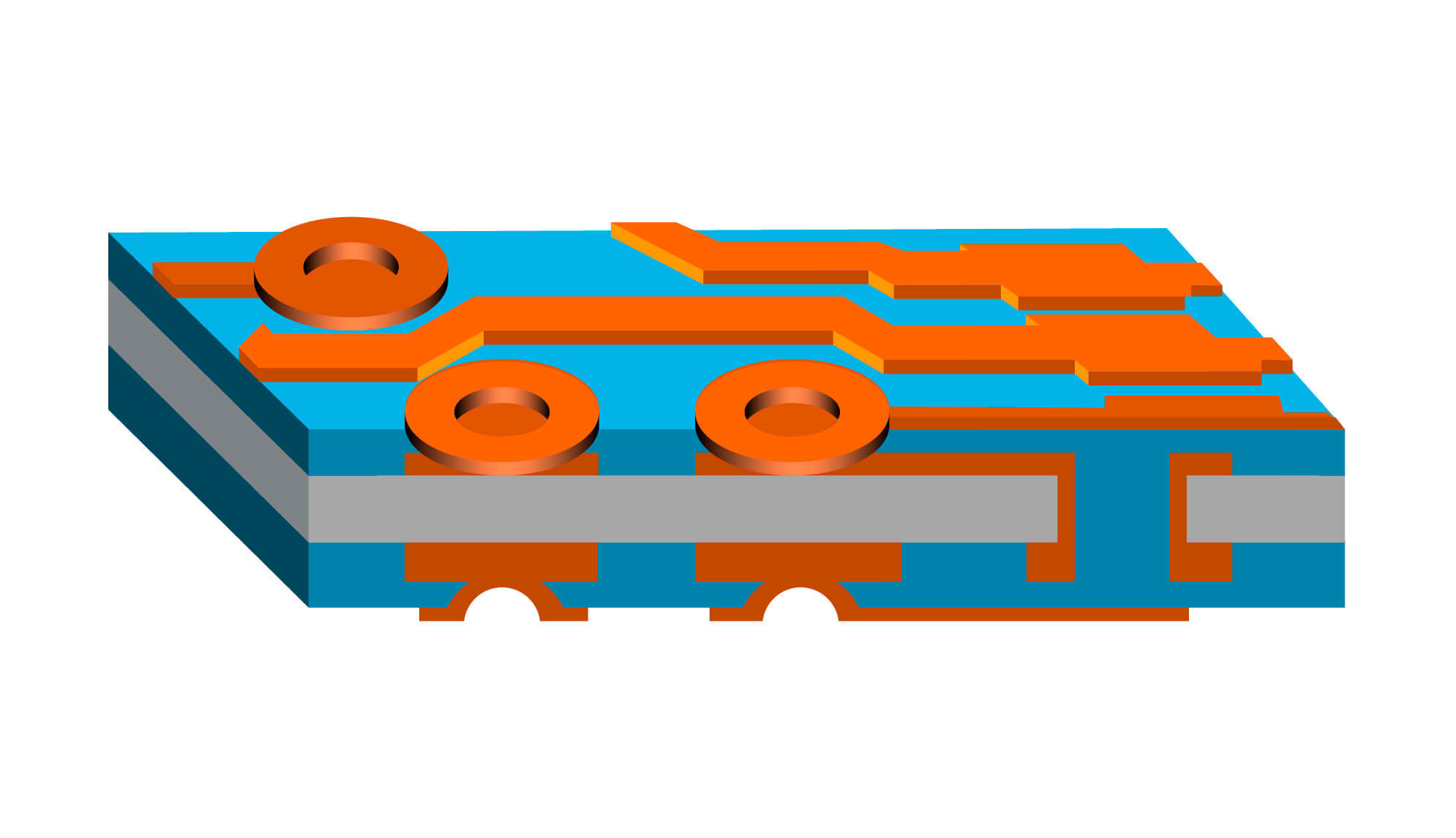
Flash etching and annealing processes are used to create the final circuitry pattern on the substrate and define its electrical functionality. The flash etch is a technique used to remove the seed layer curing the ABF layer to finalize the desired circuitry pattern. It defines the performance of the substrate for subsequent manufacturing steps and the functionality of the integrated circuitry.
Conclusion: How IC Substrate Manufacturers Can Win in a Yield-Critical Industry
The scaling of interconnect geometry throughout the semiconductor ecosystem offers an opportunity to integrate process and process control methodologies across the three worlds of front end, packaging and substrate. IC substrate manufacturers will need to adopt new strategies for yield improvement as they ramp up production of more complex ICS technology.
To start, manufacturers need advanced process tools capable of the types of processes described above as the complexity continues to increase. Then to help provide the feedback required to continuously increase yield, they must implement stringent inspection and metrology procedures for identifying and eliminating defects, as well as maintaining tight control of the process parameters at various steps of production. Manufacturers can win by minimizing waste and delivering more high-quality substrates faster to customers.
Finally, collaboration across the electronics ecosystem is a key to success. Engaging in collaborative relationships between ICS manufacturers, designers and equipment suppliers can lead to better understanding of their specific needs and requirements. By actively involving designers and equipment suppliers in the manufacturing process, manufacturers can align their efforts to deliver substrates that meet or exceed customer expectations. This collaborative approach enhances both yield and customer satisfaction and can lead to long-term partnerships.
To learn more about KLA’s solution for IC Substrate production, click here.
Follow Us