For 40 years our broadband plasma (BBP) patterned wafer inspectors have been at the forefront of defect discovery for the semiconductor industry. Introduced in 1984 and still going strong, BBP inspectors moved defect inspection inline, transforming yield management for chip manufacturing.

Explore our BBP anniversary web page and discover how our systems and technologies have evolved through the decades to address industry challenges and inflections.
40 Years of Semiconductor Innovation
Electronics and digital experiences have undergone remarkable transformations over the past 40 years. We’ve seen bulky desktop computers replaced by laptops, tablets and smartphones with remarkable compute power. The way we find information changed from books (encyclopedias, dictionaries, phone books) to web searches to AI anticipating what we want to know. Semiconductor chips have been at the center of this continuous digital evolution, helping determine the capabilities of our electronic devices. Through innovations in device and process technologies, semiconductor manufacturers have produced chips with the power, performance and profile specifications needed for our electronic devices.
Advancements in semiconductor technology over the last 40 years include the following:
- Device design node decreased from 3000nm to less than 5nm
- Transistor technology evolved from planar to vertical architectures (finFET, gate all around (GAA))
- The number of transistors in a leading-edge processor increased from ~500,000 to >100,000,000,000 (100 billion)
- The wavelength used for lithography decreased from 436nm (G-line) to 13.5nm (EUV)
- NAND memory went from planar integration to vertical 3D NAND architectures
- Numerous process and materials innovations were introduced – CMP, copper interconnects, high K metal gates, strained transistors, and more
- Singular packaging of chips evolved to multi-chip heterogeneous integration
40 Years of Advancing Semiconductor Quality
Since their introduction, our BBP inspectors have delivered the performance needed to help chipmakers navigate the numerous challenges associated with industry inflections and advancements. Capturing critical defects helps engineers characterize and debug new processes, patterning schemes, materials and device architectures during R&D, and helps accelerate chip yield, reliability and performance during high-volume production. With the continuing advancement of semiconductor technologies, we continue to develop optical and algorithm innovations that will extend BBP’s legacy of high sensitivity inspection at optical inspection speed into the future.
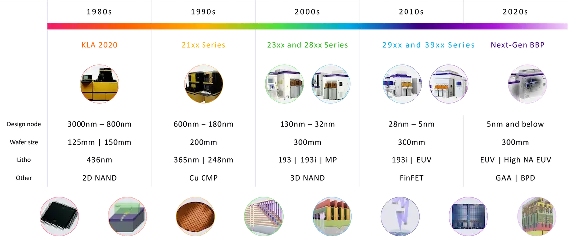
1984: KLA 2020
Introduced in 1984, the KLA 2020 was the first automated patterned wafer inspection system for chip manufacturing. The KLA 2020 replaced manual inspection by human operators using microscopes. Known as a brightfield inspector, the KLA 2020 provided fast and accurate feedback on fab processes and was primarily used for automated engineering analysis. A revolutionary process control product, the KLA 2020 transformed yield management for chip manufacturing.
1990s: 21xx Series
The 21xx Series inspectors provided the sensitivity needed for engineering analysis during R&D, supporting the characterization and integration of 200mm wafers, CMP processes and copper interconnect technologies. But it was the systems’ high speed that was the game changer: the 21xx Series inspectors introduced new sensor technology with a 100x increase in data rate compared to the KLA 2020. With this speed, the 21xx Series systems were fast enough to make inline monitoring a reality for chip manufacturing.
2000s: 23xx and 28xx Series
The 23xx Series utilized broadband ultraviolet (UV) illumination technologies to help chip manufacturers tackle the challenges associated with production adoption of copper for interconnects, the reduction of design nodes to 100nm and the transition to 300mm wafers during the first half of the decade.
Introduced in 2005, the 2800 inspector added deep ultraviolet (DUV) wavelengths, creating a DUV/UV/visible broadband inspector that captured smaller critical defects and the wide range of defect types associated with the transition to 193nm immersion lithography, which extended design nodes below 65nm.
The 283x inspectors were the first to use a laser-pumped plasma light source. The name for this illuminator – broadband plasma or BBP – became the name of this unique class of patterned wafer inspection systems.
2010s: 29xx and 39xx Series
From the 290x to the 296x, the 29xx Series systems have been the inspection workhorse of the industry since the early 2010s. Using visible/UV/DUV wavelength bands, the 29xx Series inspectors discover design and process systematic defects during R&D and capture critical layer excursions during high-volume production. The latest generation system is the 2965, which helps logic/foundry chip manufacturers ramp and produce leading-edge chips, such as GPUs for AI applications. The 2965 also features a unique wavelength band that has enabled capture of critical nanosheet defects for early development of gate all around (GAA) transistor architectures. Currently under evaluation by our customer partners, our next-generation BBP platform includes new technologies that extend nanosheet defect detection capability, making it well suited to help with ramp and production of GAA architectures.
Introduced in 2016, the 39xx Series inspectors are a technological powerhouse, utilizing a broadband wavelength range known as super resolution DUV (SR-DUV) along with the associated advanced optics, sensors and algorithms. The 39xx inspectors continue the BBP legacy of utilizing sensitivity at speed to provide full wafer defect coverage and their unique wavelengths have been essential for the discovery of critical defects for advanced nodes. In addition to supporting yield-limiting defect capture, the latest generation 3935 and 3920 EP include wavelength bands that make them particularly suited for EUV lithography quality control applications, including print check for reticle requalification and after-develop inspection (ADI).
2025 and Beyond: Next-Gen BBP
Our global team of scientists and engineers continue to develop light source, sensor, optics, data processing and algorithm innovations that will extend current BBP platforms and produce new platforms. These multiple optical patterned wafer inspectors will provide the defect discovery capability needed to support future industry challenges and inflections. The future is bright for BBP!
Read more about the evolution of KLA’s BBP technology here, and revisit 40 years of KLA innovation here.
Follow Us