The Solder Mask Application Process Is Evolving
As printed circuit board (PCB) technology progresses, the solder mask process must adapt to new and evolving demands, including the increasing complexity of PCB design, the use of new materials and compliance with environmental regulations like RoHS and REACH.
These new requirements present the challenge of reducing process costs without compromising quality and performance. Consequently, PCB manufacturers are increasingly looking for solder mask solutions that not only meet technical specifications but also enhance cost efficiency. (KLA is exhibiting at the 25th anniversary of IPC Apex Expo in March 2025.)
Market demand for increased efficiency and flexibility is driving the evolution of the solder mask application process. Meeting materials and energy efficiency requirements without compromising performance poses a significant hurdle. Manufacturers must also balance cost-effectiveness with the need for advanced technologies to keep up with rapid industry changes.
Why Inkjet for PCB Solder Mask?
While traditional methods – other than direct imaging – remain effective for high-volume production, they often involve lengthy processes with multiple steps, leading to increased production time and potential material waste. Additionally, they may lack the precision required for intricate circuit designs, resulting in less reliable outcomes.
In contrast, advanced methods like inkjet technology are well-suited to meeting these evolving requirements, offering a streamlined, resource-efficient and precise alternative. Inkjet printing is a game-changer for solder mask applications, addressing many traditional methods’ limitations.
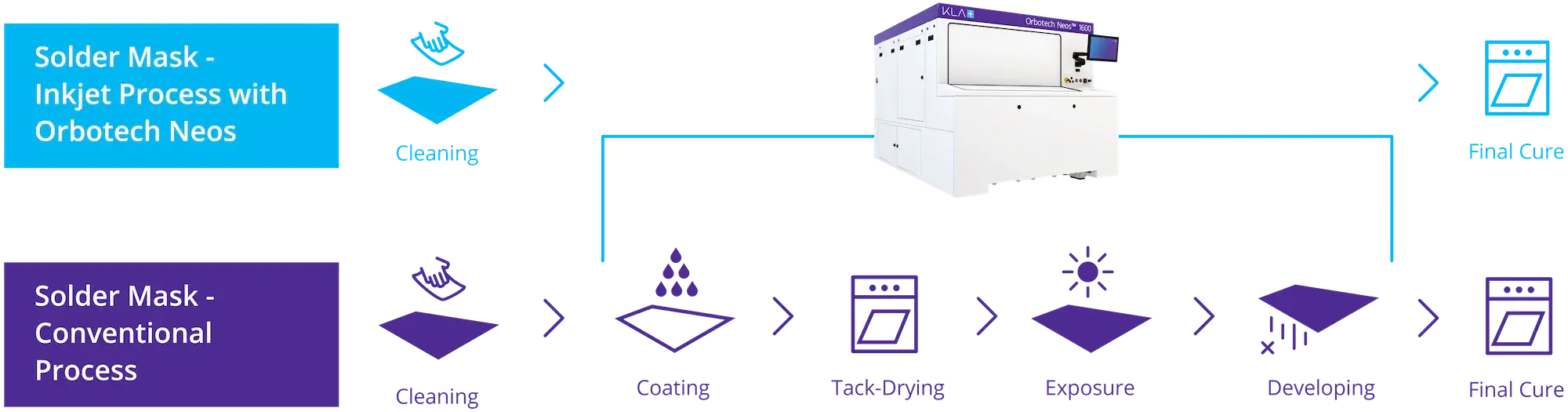
The inkjet process simplifies solder mask application by reducing steps (no coating, imaging or development) and minimizing waste, making it faster, more precise and energy-efficient than the conventional process.
KLA’s Orbotech Neos™: Solder Mask Process Streamlining Step by Step
The Orbotech Neos™ inkjet solution revolutionizes the traditional solder mask application workflow by eliminating multiple time-consuming and resource-intensive steps. Below is a comparison of solder mask application process steps, conventional vs. inkjet.
1. Data Preparation
The PCB solder mask process begins with preparing the necessary design files and verifying they are accurate and complete. The data includes the layout of the PCB, the areas to be masked, and the areas to be left exposed for soldering.
Traditionally, PCB design is prepared using CAM/CAD software to generate photo tools or direct imaging (DI) files for defining the solder mask pattern.
Using inkjet, CAM data is prepared digitally for inkjet printing, eliminating the need for photo tools. The digital workflow integrates directly with the printer. CAM data are loaded and used to print the pattern by inkjet.
2. Pretreatment – Surface Cleaning/Preparation
Contaminants, oxidation and residues must be removed thoroughly from PCB surfaces. For proper adhesion of the solder mask to the PCB surface, the PCB surface is usually cleaned or prepared mechanically or chemically. In either case, mechanical processes such as brushing, pumicing, jet scrubbing or chemical processes like microetching are used.
With inkjet, the PCB surface is also cleaned/prepared so it adheres properly to the solder mask. For improved solder mask printing quality, a surfactant needs to be applied.
3. Coating
During conventional, full-surface coating, solder mask is applied across the entire PCB using screen printing or curtain coating or spray coating. The mask material is typically a liquid photoimageable (LPI) epoxy. This results in excess solder mask material that will later be removed during the development stage.
Efficient application techniques and proper handling can improve material efficiency. Using inkjet, application is selective. Solder mask material is applied only to the required areas. Solder mask by inkjet optimizes the use of materials to reduce waste and cost.
4. Pre-Cure
After application, the solder mask undergoes a soft curing step (via heat) to partially consolidate the coated solder mask before imaging. This step helps stabilize the mask for the subsequent exposure process.
Using inkjet, no pre-drying is needed. Inkjet printing eliminates the need for soft curing since the material is cured directly during application.
5. Exposure/Imaging
The PCB is exposed to UV light through a photomask that defines the areas to be hardened. The exposed areas of the solder mask become polymerized and harden, while the unexposed areas remain soft.
Using inkjet, the imaging step is unnecessary. The inkjet printer directly applies and cures the solder mask pattern digitally, eliminating this step entirely.
6. Development
The unexposed, soft areas of the solder mask are washed away using a developer solution – typically a mild alkaline solution – leaving only the hardened areas. This step reveals the copper pads and traces that need to be soldered.
Inkjet application directly deposits the solder mask where needed, skipping chemical development entirely.

7. Post Curing
Thermal curing is used to harden the solder mask for durability and adhesion.
With inkjet, similar thermal curing is used for final hardening.
Recap: The Benefits of Solder Mask by Inkjet
| Process Step | Conventional | Inkjet |
|---|---|---|
| Coating | Full-surface coating; excess material | Selective, precise application |
| Pre-Cure | Required | Not required |
| Exposure / Imaging | Required | Not required |
| Development | Required | Not required |
| Material Efficiency | High material waste | Minimal material usage |
| Process Complexity | Multi-step, labor-intensive | Streamlined and efficient |
| Process Cost | High operational cost (multiple tools) | Low operational cost (one tool) |
PCB manufacturers should explore inkjet solutions like Orbotech Neos to stay competitive in today’s market, where precision and flexibility are critical to success. To learn more contact us.
Follow Us