We sat down with Oreste Donzella, who explains how innovation is diversifying in the semiconductor chip industry, resulting in new approaches to meet the performance needs of advanced technologies like artificial intelligence.
Innovation in semiconductor content has largely followed Moore’s Law. Is this changing?
The fundamental goals remain the same – improved performance, power and cost efficiency. But the semiconductor technology roadmap is evolving with innovation beyond traditional geometric scaling.
In my career, I’ve seen quite a bit of technology node scaling. Where we used to measure geometries in microns, we now measure in nanometers, and we’re looking ahead to angstroms. Technology made huge progress in the ability to scale the densities of the devices and the number of transistors. Looking back, we have seen the industry pack twice the number of transistors in the same-sized piece of silicon every 18 to 24 months or so according to Moore’s prediction, driven primarily by advancements in lithography.

Oreste Donzella is executive vice president and chief strategy officer at KLA.
What’s happening now in the evolution of chip technologies?
The cycle has begun to slow down and has become more expensive.
And as transistor counts rise, the complexity of semiconductor connectivity also rises. Going forward, we see innovation diversifying. Conventional scaling is still happening with high NA EUV (numerical aperture extreme ultraviolet) lithography and new transistor architectures like gate all around (GAA), with a shift to backside power distribution networks (BPDN) to help reduce power consumption. But going forward, non-traditional areas such as semiconductor packaging will play a more crucial role in driving performance, power, connectivity and cost advancements.
How are these benefits achieved in packaging?
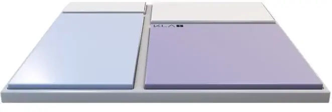
Packaging used to be simply about protecting and connecting individual semiconductor chips. Now, the key to advanced packaging is heterogeneous integration, where multiple functions originating from different chip technologies are integrated together in a single package. Designers mix and match individual chips – sometimes referred to as chiplets – like building blocks to gain greater overall system performance at lower cost.
Innovative packaging technologies invite new ways to add more functions and optimize interconnect densities, bringing chip functions physically closer together to unlock computing, latency and power advantages.
We are moving from a “system on a chip” to a “system of chips” concept through a disaggregation of functions previously built on a single die.
Can you give an example of how heterogeneous integration is being applied?
Today’s advanced graphics processing units (GPUs) are a great example of how heterogeneous integration makes possible the high-performance architecture that’s essential for delivering AI-caliber computing power.
A decade ago, GPU memory might have topped out at 12GB. Today we’re approaching 192GB achieved through high-bandwidth memory (HBM) – DRAM (dynamic random access memory) chips stacked on top of each other. Using advanced packaging, GPU packages are integrating GPU processor chips and multiple stacked HBM memory modules in close proximity inside the same package.
The compute performance enabled with this architecture is crucial for powering AI-era workloads.
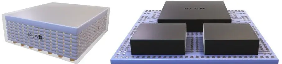
Left, high bandwidth memory (HBM) stack. Combining processor and HBM modules (right) into one package.
Where is packaging technology headed?
Going forward, there are infinite potential combinations for heterogeneous integration architecture in packaging that can be innovated in the next five to 10 years, provided the economics are favorably aligned. KLA offers solutions that help semiconductor manufacturers build these advanced devices efficiently with high quality and yield.
What role does heterogeneous integration play in keeping production costs down?
The performance benefit for heterogeneous integration made itself known with the advent of the system on chip (SoC) concept many years ago.
At the time, leading central processing unit (CPU) producers achieved the ability to add multiple functions on the same wafer, on the same chip, all interconnected. The problem with this approach is that you may require an advanced technology node wafer like 3nm for the processor chip, for example, but there will be other functions like input/output (I/O) circuitry, DRAM memory controllers and temporary SRAM (static random access memory) cache storage chips that don’t need to be implemented at 3nm. In those scenarios, you’re wasting valuable 3nm wafer space on functions that could be implemented much more cost effectively.
Heterogeneous integration has emerged as the most cost-effective way to integrate multiple functions in packaging instead of on a wafer, with the requisite performance, power distribution and interconnect density.
How are these higher interconnect densities achieved, and what’s driving the demand?
We continue to see acceleration of heterogeneous integration with new 2.5 and 3D architectures serving various end-applications, including high-performance computing (HPC), mobile and networking, among others.
The proliferation of AI is a major driver, particularly as it expands beyond the cloud hyperscaler domain to encompass mobile and edge devices in the years ahead – all of which require a high quantity of semiconductor content and advanced packaging technologies.
The industry is developing new ways to achieve high interconnect density to meet performance and costs requirements, including hybrid bonding, embedded bridges, wafer and panel interposers, glass core substrates and, in the longer term, co-packaged optics. Different packaging technologies will continue to be deployed as the approach is dictated by the specific needs of the end market, unlike front end wafer fabrication where it is more standardized.
Is the industry and KLA prepared to meet production challenges?
Each of these heterogeneous integration methods will bring new process and process control challenges across wafer-level packaging, assembly and substrate manufacturing. KLA’s combined expertise in front end semiconductors, packaging and IC substrates will help customers achieve breakthroughs in packaging interconnect density for chips targeting high-performance apps.
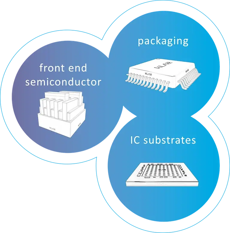
There is significant opportunity to bridge methodologies across the three worlds of front end, packaging and substrates. These once completely separated domains are becoming integrated just like the packages and systems they create.
As a result of the more complex packaging manufacturing requirements, we see an increasing demand for more advanced inspection and metrology solutions, which can derive directly from front end semiconductor, with some packaging-specific customization mostly related to handling and algorithms.
Similarly, heterogeneous integration is introducing new architectures and integration flows, requiring process optimizations that have never been needed in packaging before. The introduction of new process applications, such as low contact resistance (Rc) barrier seed sputtering, thick oxide CVD deposition and plasma dicing, play to the strengths of our SPTS wafer processing systems.
Finally, many of the advancements achieved in packaging will target the substrate and panel-level, where KLA applies our product portfolio and expertise in the PCB market. KLA’s strategic vision for this technology is coming to fruition, and we’ll be sharing more about our plans for IC substrates and panel-based technologies in the months ahead.
What’s KLA’s role in driving advanced semiconductor packaging yield?
There is a pervasive infusion of semiconductors in everyday life today, particularly as AI takes hold. We’ve arrived at the “Digitization of Everything” era, where AI is starting to drive the ecosystem in ways we haven’t seen before. This means that semiconductor content will continue to grow – it’s a growth industry. KLA is very well positioned in packaging technology, and our combined expertise in front end semiconductors, packaging and IC substrates is unique in the industry and is valuable for our customers.
There are many challenges affecting 2.5D and 3D packaging, and KLA plays an important role in overcoming them. We’re bringing the precision of front end semiconductor manufacturing to the dynamic realm of customized packaging. Customers today want increasingly high sensitivity for inspection in packaging, customized to account for different handling, noise sources, warpage and thicknesses found in packaging applications. They need front end-like inspection and metrology capabilities and KLA provides them.
Manufacturers who have benefited from KLA’s AI-driven data analytics in front end wafer production are hugely enthusiastic to see this technology applied in packaging. KLA pioneered a way for semiconductor wafer fabs to collect and analyze data and enhance processes in a feedback correction loop based on the data collected from their inspection and metrology tools. KLA brings integrated software analysis and AI to the table in a way that provides unique insight to continuously drive yield and value.
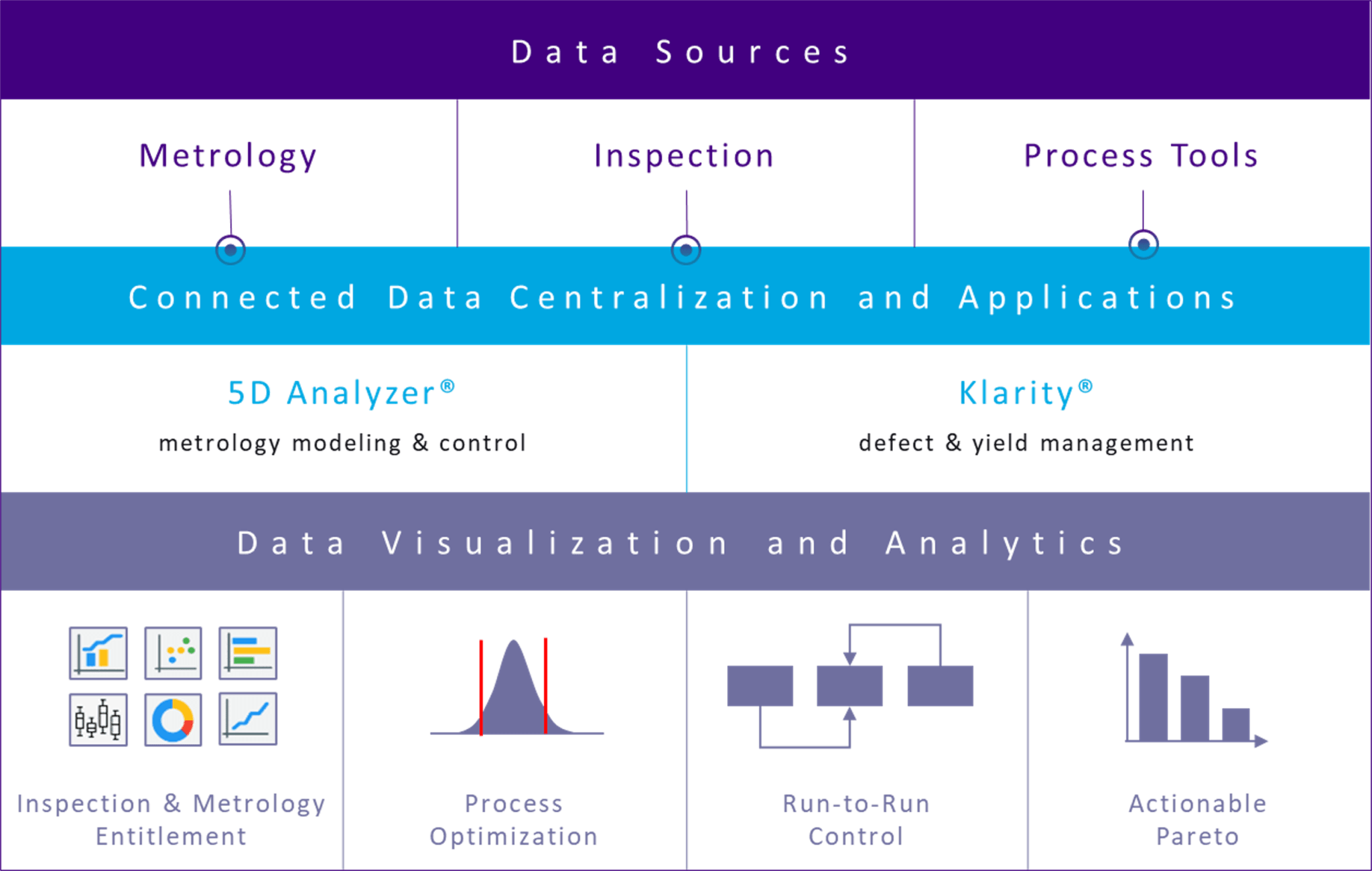
KLA’s software solutions for the semiconductor ecosystem centralize and analyze the data produced by inspection, metrology and process systems to provide actionable information for manufacturers to accelerate yield and reduce production risk.
KLA offers the tools and the data analytics to help customers capitalize on the massive opportunity emerging in advanced semiconductor packaging. It’s truly an exciting time for the industry.
Follow Us