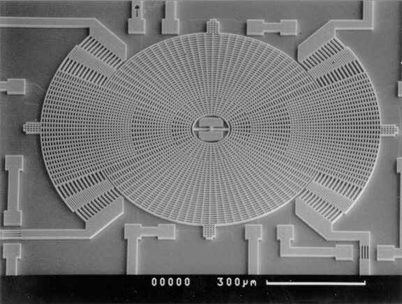
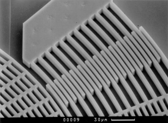
Micro Electromechanical Systems (MEMS), for anyone that is not familiar with the term, are micromachines which convert movement into an electrical signal, or electrical power into motion. The field is often expanded to also include various microfluidic devices. They are typically made of silicon which is widely available, inexpensive and allows easy integration into electronic circuits, although some MEMS or components within the system may be made of glass, ceramics, polymers or metals.
The earliest MEMS developed from emerging silicon integrated circuit (IC) technology in the late 1960s, in the form of resonant gate transistors, and a range of microsensors for pressure, motion, chemical or light. Most depended on wet anisotropic etching to micromachine bulk single crystal silicon to form 3D geometries, including diaphragms, beams, masses, grooves and holes at the micrometer scale.
Development of The Bosch Process
SPTS (at the time known as Surface Technology System, or STS) joins the story in the mid-1990s when we were approached by researchers from Robert Bosch GmbH to industrialize a new dry plasma etch technology which Bosch had invented to overcome the limitations of wet and standard inductively coupled plasma (ICP) etching. This new “Bosch Process” (also known as deep reactive ion etching – DRIE) enabled the anisotropic etching of extremely deep, high aspect ratio, and vertical features into the silicon wafer, independent of crystal orientation. Initially, the primary driver for Bosch was to create gyroscopes and accelerometers for automotive safety applications, but ultimately this joint development was a critical development in the story of manufacturing a whole host of MEMS devices, as the deal struck with Bosch allowed SPTS to sell their new silicon etch system to other device manufacturers making everything from inkjet heads to optical MEMS. In 2007, Franz Lärmer and Andrea Urban, the inventors from Bosch, were named as European Inventors of the Year[1] in recognition of the revolutionary impact their DRIE process had made in advancing MEMS technology.
As a co-developer of the technology, SPTS had an exclusive license to offer the Bosch Process in their plasma etch portfolio and continued to improve the capabilities of their equipment. For more than 25 years, SPTS has developed unrivalled wealth of silicon etching expertise which has continued to push the limits of this etch technology over the past decade. Since 1995, the company has sold nearly 1,500 DRIE modules, and now as a KLA company continues to supply virtually all the top MEMS manufacturers and foundries involved in making a vast array of sensors, actuators and microfluidic devices. End applications include areas such as smart agriculture, factory automation, biomedical devices, home entertainment, microphones and smartphones.
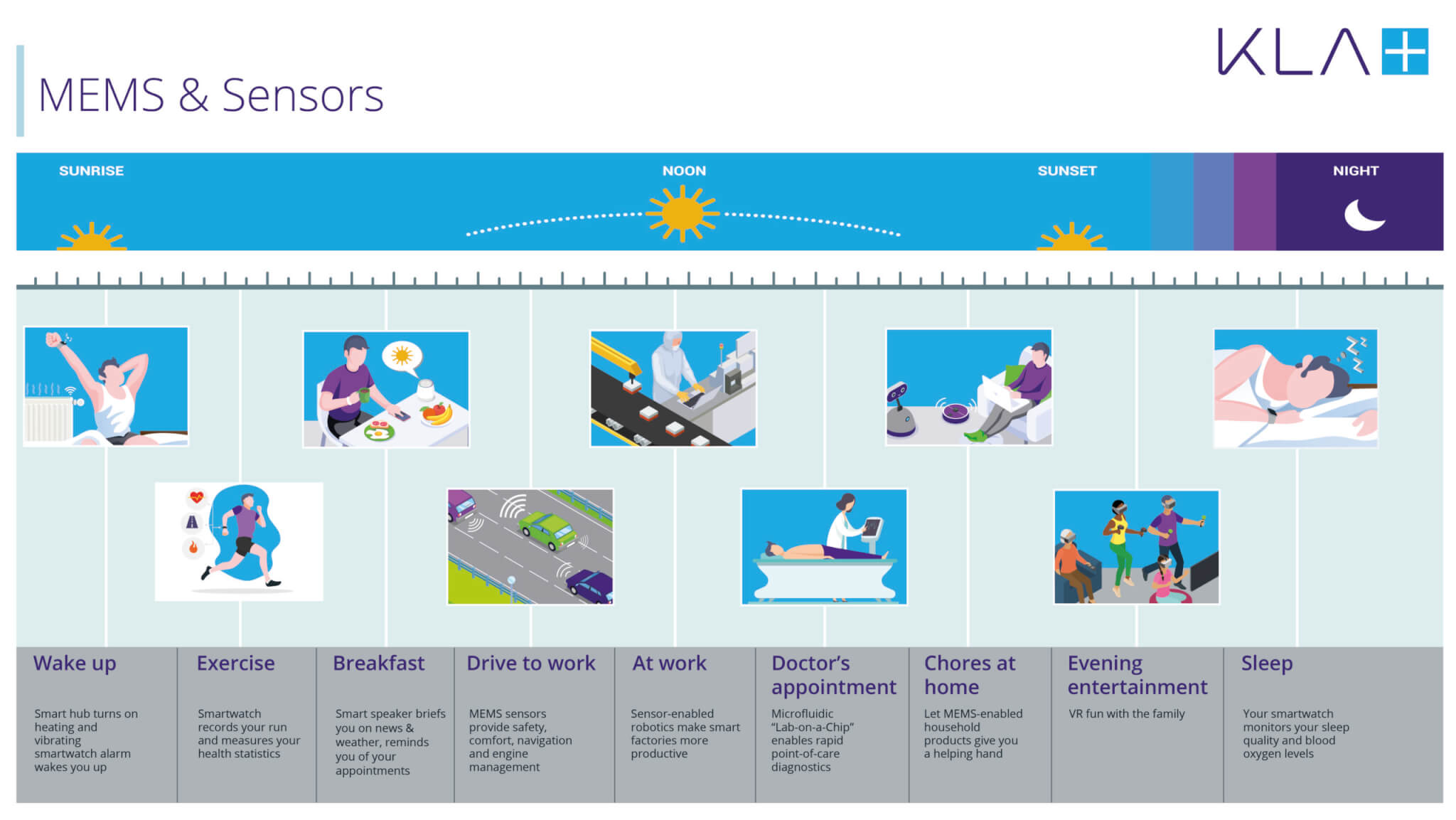
The infographic shows how MEMS and sensors now touch our lives in many ways, every day.

Other SPTS Processes for MEMS Manufacturing
During the first half of 2021, SPTS has experienced an increase in our MEMS business destined for manufacturing devices for automotive applications. This includes not only silicon etch systems, but also PVD and PECVD systems, which can be used to deposit metals, AlScN or dielectrics layers used in the MEMS structures.
Vapor release etch processes also play a significant role in MEMS manufacturing, using vapor HF or XeF2 to remove sacrificial oxide or silicon layers to release moving components without stiction or corrosion commonly associated with wet etching solutions.
Automotive MEMS Market Outlook
In May 2020, Yole estimated that automotive MEMS market will rebound (after COVID) to be worth $2.6 billion by 2025 (CAGR of 3%), representing around 15% of the total MEMS market[2], with pressure and inertial sensors for safety systems such as tire pressure sensors airbags, electronic safety control (ESC) and roll-over detection continuing to be the main applications. Looking further, Emergen Research forecasted a higher CAGR for automotive MEMS sensors of 14.1% from $1.79 billion in 2019 to $4.84 billion in 2027 stimulated by the growing adoption of electric vehicles, inter-vehicle communication and advanced driver-assistance systems (ADAS)[3].
Summary
Working closely with our customers has always helped SPTS ensure we continue to develop the right processes that meet the future needs of the semiconductor industry, and identify new applications where our technology can offer real benefits in terms of manufacturing costs and yield. The co-development of deep silicon etch process is a prime example of how listening to our customers’ ideas, recognizing the potential of the emerging MEMS market in the 1990s and using our expertise to develop the technology has led to sustainable growth for both SPTS and our customers.
[1] https://www.epo.org/news-events/events/european-inventor/finalists/2007/laermer.html
[2] https://www.yole.fr/iso_upload/News/2020/PR_STATUS_MEMS_INDUSTRY_MarketUpdate_YOLEGROUP_July2020.pdf
[3] https://www.emergenresearch.com/industry-report/automotive-mems-sensor-market
Follow Us

